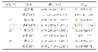
《表1 In P基p HEMT外延材料结构》
 提示:宽带有限、当前游客访问压缩模式
本系列图表出处文件名:随高清版一同展现
《D波段InP基高增益低噪声放大芯片的设计与实现(英文)》
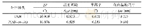
The backside of InP HEMT MMIC process provides a 50-um-thick wafer for reduce the high frequency loss with through substrate vias,which connect the backside metal ground plane to the front side device and circuit elements.Additionally,30μm diameter through-substrate vias are used for minimizing source inductance and maintaining high device gain.The process further includes 50Ω/sq Ni Cr thin film resistors(TFRs),0.3 f F/μm2metal-insulator-metal(MIM)capacitors,and thrusubstrate vias.
| 图表编号 | XD0034302400 严禁用于非法目的 |
|---|---|
| 绘制时间 | 2019.04.01 |
| 作者 | 刘军、吕昕、于伟华、杨宋源、侯彦飞 |
| 绘制单位 | 北京理工大学毫米波与太赫兹技术北京市重点实验室、北京理工大学毫米波与太赫兹技术北京市重点实验室、北京理工大学毫米波与太赫兹技术北京市重点实验室、北京理工大学毫米波与太赫兹技术北京市重点实验室、北京理工大学毫米波与太赫兹技术北京市重点实验室 |
| 更多格式 | 高清、无水印(增值服务) |
