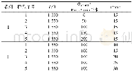
《Table 1.Some works on etch rate and etch surface RMS of GaN.》
 提示:宽带有限、当前游客访问压缩模式
本系列图表出处文件名:随高清版一同展现
《Implementation of slow and smooth etching of GaN by inductively coupled plasma》
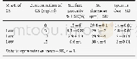
ΔRMS=RMS(after etching)–RMS (before etching)
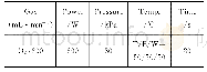
Four sets of experiments were conducted to study the effect of etching process parameters of ICP power,RF power,flow rate of Cl2 and BCl3 on the etch rate(ER)and etch surface roughness(RMS),respectively.The detailed etching parameters for different samples are listed in Table 2.All etching processes were performed at 8 mTorr chamber pressure,5 sccm Ar and etch time 250 s.Then put all etched samples into the splitter to remove the photoresist.Finally,the groove structures were measured by AFM to give out the etch rate and RMS roughness.The scanning area is 20×20μm2.
| 图表编号 | XD00188453200 严禁用于非法目的 |
|---|---|
| 绘制时间 | 2018.11.01 |
| 作者 | Xilin Li、Ping Ma、Xiaoli Ji、Tongbo Wei、Xiaoyu Tan、Junxi Wang、Jinmin Li |
| 绘制单位 | Research and Development Center for Solid State Lighting, Institute of Semiconductors, Chinese Academy of Sciences、University of Chinese Academy of Sciences、Beijing Engineer Research Center for the 3rd Generation Semiconductor Materials and Application、Re |
| 更多格式 | 高清、无水印(增值服务) |


