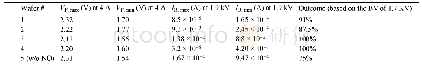
《Table 3.Summary of the forward voltage drop (VF) and the reverse blocking voltage (VR) obtained fro
 提示:宽带有限、当前游客访问压缩模式
本系列图表出处文件名:随高清版一同展现
《Impact of design and process variation on the fabrication of SiC diodes》
Initially,we will discuss the electrical characteristics of4 A diodes.All the measurements are done at room temperature.In Table 1,different design variations used to fabricate the diodes are listed.In total,diodes with three different stripe designs(d1–d3)and 5 segments designs(d4–d7)have been fabricated.
| 图表编号 | XD00188454500 严禁用于非法目的 |
|---|---|
| 绘制时间 | 2018.11.01 |
| 作者 | Y.K.Sharma、Huaping Jiang、Changwei Zheng、Xiaoping Dai、Yangang Wang、I.Deviny |
| 绘制单位 | Dynex Semiconductor Ltd、Dynex Semiconductor Ltd、Zhuzhou CRRC Times Electric Co.Ltd.、Dynex Semiconductor Ltd、Zhuzhou CRRC Times Electric Co.Ltd.、Dynex Semiconductor Ltd、Zhuzhou CRRC Times Electric Co.Ltd.、Dynex Semiconductor Ltd、Dynex Semiconductor Ltd |
| 更多格式 | 高清、无水印(增值服务) |

