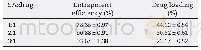
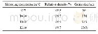
《Table 2Apparent quantum efficiencies of the different samples.》
 提示:宽带有限、当前游客访问压缩模式
本系列图表出处文件名:随高清版一同展现
《CuO和Au纳米结构协同增强Cu_2O立方体光催化活性和稳定性(英文)》
Note:Apparent quantum efficiency was defined as[29,30]:Φ=K/S,where K is the photo‐degradation rate of MO,S is the area used for the convolution of the irradiance of the light source with the UV‐vis diffuse reflection spectrum of the samples at 400≤
To explore surface states of the Cu2O etched by EDA,XPS spectra of Au/CuO/Cu2O were compared with those of pristine Cu2O and Cu O/Cu2O,as shown in Fig.2(A)and Table 1.The peaks at 932.2 and 934.1 e V were attributed to Cu(I)and Cu(II),respectively[27].Compared to pristine Cu2O,the Cu(I)peak shifted slightly to a lower binding energy.As shown in Table 1,the surface area ratio of Cu(II)to Cu(I)of the as‐obtained Au/Cu O/Cu2O was compared to those of pristine Cu2O and Cu O/Cu2O.The ratio of Cu(II)to Cu(I)of the Au/Cu O/Cu2O material was only slightly higher than that of pristine Cu2O.Combined with the SEM results,these results indicate that most Cu(II)came from the CuO polyhedron rather than the CuO film formed under ambient conditions.It also suggests that most of the naturally‐grown CuO film was removed.It should be noted that naturally‐grown CuO thin films on Cu2O cubes act as a bar‐rier layer preventing charge transfer in the Cu2O cubes[2,4,5].
| 图表编号 | XD0028864400 严禁用于非法目的 |
|---|---|
| 绘制时间 | 2019.01.01 |
| 作者 | 蒋登辉、张跃钢、李鑫恒 |
| 绘制单位 | 中国科学院兰州化学物理研究所羰基合成与选择氧化国家重点实验室和苏州研究院、中南大学资源加工与生物工程学院、中国科学院苏州纳米技术与纳米仿生研究所国际实验室、中国科学院兰州化学物理研究所羰基合成与选择氧化国家重点实验室和苏州研究院 |
| 更多格式 | 高清、无水印(增值服务) |