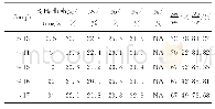
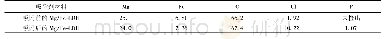
《表3 B2H6通气后钨薄膜表面元素原子数分数的XPS结果》
 提示:宽带有限、当前游客访问压缩模式
Fig.13(a)clearly shows that there are no voids left after the bulk W deposition with the N treatment on the structure wafer,while the voids can be clearly seen in the case of the traditional CVD W deposition,which is shown in Fig.13(b).It suggests that the N plasma treatment is a promising fashion to solve the W gap fill void in the contact or via with high aspect ratio.
| 图表编号 | XD0083679100 严禁用于非法目的 |
|---|---|
| 绘制时间 | 2019.11.15 |
| 作者 | 张念华、万先进、李远、许爱春、潘杰、左明光、胡凯、詹侃、宋锐、毛格、彭浩、李晓静、闫薇薇、曾传滨 |
| 绘制单位 | 中国科学院微电子研究所、长江存储科技有限责任公司、中国科学院大学微电子学院、中国科学院硅器件技术重点实验室、长江存储科技有限责任公司、长江存储科技有限责任公司、长江存储科技有限责任公司、长江存储科技有限责任公司、长江存储科技有限责任公司、长江存储科技有限责任公司、长江存储科技有限责任公司、长江存储科技有限责任公司、长江存储科技有限责任公司、长江存储科技有限责任公司、中国科学院微电子研究所、中国科学院硅器件技术重点实验室、中国科学院微电子研究所、中国科学院硅器件技术重点实验室、中国科学院微电子研究所、中国科 |
| 更多格式 | 高清、无水印(增值服务) |

