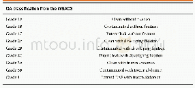
《Table 1 Binary truth table of the logic gate.Reprinted from ref.[23], with the permission of AIP Pu
![《Table 1 Binary truth table of the logic gate.Reprinted from ref.[23], with the permission of AIP Pu](http://bookimg.mtoou.info/tubiao/gif/JGXG201904002_16500.gif) 提示:宽带有限、当前游客访问压缩模式
提示:宽带有限、当前游客访问压缩模式
本系列图表出处文件名:随高清版一同展现
《Nanoscale all-optical logic devices》
When the ring is at resonance,optical forces cause the freehanging parts to bend downwards,as shown in Figure 6(b)This bending deformation can cause a change in the optica path length that leads to a red-shift in the resonant wavelength,which then affects all the optical modes in the ben rings.Therefore,the output transmission of the probe lightλc is modulated by this resonance shift;as a result,the outpu transmission of the probe light decays,which is defined as the logic“0”.In another situation withoutλaandλb,the probe light cannot resonate with the microrings and the transmission remains relatively high.This state is defined as the logic“1”.The binary truth table for this logic gate is shown in Table 1.The advantages of this logic gate include its low power consumption(approximately 0.5 mW)and its highly compact size(40μm×45μm).
| 图表编号 | XD0052895000 严禁用于非法目的 |
|---|---|
| 绘制时间 | 2019.04.01 |
| 作者 | Ye Chen、YinKe Cheng、RongBin Zhu、FeiFan Wang、HaoTian Cheng、ZhenHuan Liu、ChongXiao Fan、YuXuan Xue、ZhongCheng Yu、JianKun Zhu、XiaoYong Hu、QiHuang Gong |
| 绘制单位 | State Key Laboratory for Mesoscopic Physics & Department of Physics, Collaborative Innovation Center of Quantum Matter, Peking University、State Key Laboratory for Mesoscopic Physics & Department of Physics, Collaborative Innovation Center of Quantum Matte |
| 更多格式 | 高清、无水印(增值服务) |
查看“Table 1 Binary truth table of the logic gate.Reprinted from ref.[23], with the permission of AIP Publishing”的人还看了
-

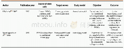
- Table 2 Studies retrieved from PubMed database evaluating the effect of DPSCs on nerve repair or regeneration in-vivo
-

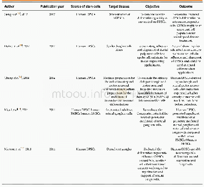
- Table 3 Studies retrieved from PubMed database evaluating the effect of DPSCs on nerve repair or regeneration in-vitro
