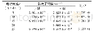
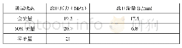
《表3 双异质结的有效载流子寿命》
 提示:宽带有限、当前游客访问压缩模式
本系列图表出处文件名:随高清版一同展现
《InGaAsP/InGaAs双结太阳电池的开路电压损耗抑制(英文)》
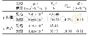
It is well established that SL serve as effective barrier for element diffusion or intermixing,and dislocation threading,and it has been widely used in semiconductor devices such as high electron mobility transistors,laser diodes,electro absorption modulators[12-16].Also,the miniband in SL would not introduce extra potential barrier for carrier transport[17].An initial five-period InP(2nm)/InAlAs(2nm)SL BSF layer is designed and employed in bottom InGaAs subcell of DJSC.A Vocof 997.5mV,a Jsc of 15.8 mA/cm2and an FF of 0.824 are obtained as in Fig.8.Both Vocand Jsc are boosted,as expected,in fabricated SL BSF device.The Vocapproaches1.0 V,resulting in a Woc of 752.5 mV.A reduction of30 mV in Vocloss for DJSC is achieved,compared with the conventional InP BSF DJSC.
| 图表编号 | XD00199653700 严禁用于非法目的 |
|---|---|
| 绘制时间 | 2021.02.01 |
| 作者 | 陆宏波、李欣益、李戈、张玮、胡淑红、戴宁、杨瑰婷 |
| 绘制单位 | 中国科学院上海技术物理研究所红外物理国家重点实验室、上海空间电源研究所空间电源技术国家重点实验室、中国科学院大学、上海空间电源研究所空间电源技术国家重点实验室、上海空间电源研究所空间电源技术国家重点实验室、上海空间电源研究所空间电源技术国家重点实验室、中国科学院上海技术物理研究所红外物理国家重点实验室、中国科学院上海技术物理研究所红外物理国家重点实验室、上海空间电源研究所空间电源技术国家重点实验室 |
| 更多格式 | 高清、无水印(增值服务) |
