《Tab.1 Sample layer structure》
 提示:宽带有限、当前游客访问压缩模式
本系列图表出处文件名:随高清版一同展现
《基于GaAs膜的GaInP/AlGaInP无杂质空位扩散诱导量子阱混杂的研究(英文)》
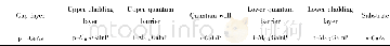
The laser structure in this work was grown on Si-doped(100)Ga As substrate with a misorientation of 10°towards(111)A by low pressure MOVPE.Epitaxial growth was carried out in an AIX200 system which contains a horizontal reactor.During the epitaxy,the growth temperature was controlled at 650-725℃and the growth pressure was about 5 000 Pa.The source materials were trimethylaluminium(TMAl),arsine(As H3)and phosphine(PH3).The p-type dopant was silane(Si H4).The carrier gas was palladium-diffused hydrogen.All layers include the following sequence from the substrates:a Si-doped 200-nm-thick n-Ga In P buffer layer,a Si-doped 1 000-nm-thick n-Al0.7Ga In P cladding layer(dopant concentration n= (5-8)×1017cm-3) ,a compressively strained single-quantum-well(SQW)structure(barrier:Al Ga In P:350nm,well:Ga In P:9 nm),a Zn-doped 1 000-nmthick Al Ga In P cladding layer(dopant concentration p= (1-2)×1018cm-3) ,and a higher p-doped contact layers(dopant concentration p= (1-2)×1020cm-3) ,including a 50-nm-thick Ga In P layer and a100-nm-thick Ga As layer.A schematic diagram of the layers'structure is given in Tab.1.The laser was designed to have a peak emission at 660 nm.Fig.1shows the photoluminescence(PL)spectrum at RT.
| 图表编号 | XD0017632700 严禁用于非法目的 |
|---|---|
| 绘制时间 | 2018.08.01 |
| 作者 | 田伟男、熊聪、王鑫、刘素平、马骁宇 |
| 绘制单位 | 中国科学院半导体研究所光电子器件国家工程研究中心、中国科学院大学材料科学与光电技术学院、中国科学院半导体研究所光电子器件国家工程研究中心、中国科学院半导体研究所光电子器件国家工程研究中心、中国科学院半导体研究所光电子器件国家工程研究中心 |
| 更多格式 | 高清、无水印(增值服务) |
