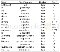
《Table 1.Instruction formats of DLX RISC》
 提示:宽带有限、当前游客访问压缩模式
本系列图表出处文件名:随高清版一同展现
《Berger code based concurrent online self-testing of embedded processors》
During the IF stage,a 32-bit instruction will get fetched from the memory.The PC holds the address of the next instruction to be fetched(i)by incrementing PC by 4 in case of sequential execution and(ii)the branch target address predicted by the branch prediction logic.During the ID stage,the instruction decoder decodes the 32-bit instructions into various fields as given in Table 1 and determines the required operands and branching address.During the EXE stage,the arithmetic logic unit(ALU)performs the arithmetic and logical operations on the operands decoded/provided by the instruction decoder.During the MEM stage,the computed results will be written back to the data memory.The result will be written back into register during the WB stage.The MEM and WB cycles can be performed in a single clock cycle and hence the execution of an instruction can be completed in 4clock cycles.
| 图表编号 | XD001113600 严禁用于非法目的 |
|---|---|
| 绘制时间 | 2018.11.01 |
| 作者 | G.Prasad Acharya、M.Asha Rani |
| 绘制单位 | Department of ECE, Sree Nidhi Institute of Science and Technology、Department of ECE, JNTUH College of Engineering, JNTUH University |
| 更多格式 | 高清、无水印(增值服务) |


