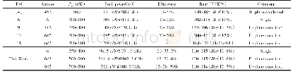
《表1 相邻频段的倍频器性能比较》
 提示:宽带有限、当前游客访问压缩模式
本系列图表出处文件名:随高清版一同展现
《大功率单路和功率合成式100~115 GHz肖特基平衡式二倍频器(英文)》
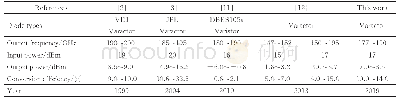
Figure 7(c)presents the test output power and conversion efficiency of combined doubler B.With the optimized bias voltage,a peak output power of 212 mW is achieved at 108.6 GHz,while the peak conversion efficiency is 28.36%at 102 GHz.And the typical value of the output power over 101~112 GHz is proved to be 150mW.Compared to the single one,efficiency of this combined doubler B has dropped by 6 percent.This can be attributed to the waveguide transmission losses introduced by the V-band splitter and D-band combiner topology applied to the doubler.Unlike doubler A,the output power curves of doubler B is much flatter and more consistent with the simulate results.This improvement is achieved by the carefully designed waveguide T-junction layout with perfect amplitude and phase balance.Also,there is a small discrepancy between simulated and measured results when it comes to the efficiency and output power.It is believed that dielectric losses of substrates and/or series resistance values of Schottky junctions used in simulations were overestimated.A summary of the comparison between these measured performances with the reported frequency doublers is listed in Table 1.
| 图表编号 | XD00199654500 严禁用于非法目的 |
|---|---|
| 绘制时间 | 2021.02.01 |
| 作者 | 田遥岭、黄昆、岑冀娜、唐川云、林长星、张健 |
| 绘制单位 | 中国工程物理研究院微系统与太赫兹研究中心、中国工程物理研究院电子工程研究所、中国工程物理研究院微系统与太赫兹研究中心、中国工程物理研究院电子工程研究所、中国工程物理研究院微系统与太赫兹研究中心、中国工程物理研究院电子工程研究所、中国工程物理研究院微系统与太赫兹研究中心、中国工程物理研究院微系统与太赫兹研究中心、中国工程物理研究院电子工程研究所、电子科技大学电子科学与工程学院 |
| 更多格式 | 高清、无水印(增值服务) |
