《数字集成电路 设计透视 英文 影印版》
| 作者 | 拉贝(Rabaey J.M.)著 编者 |
|---|---|
| 出版 | 北京:清华大学出版社 |
| 参考页数 | 706 |
| 出版时间 | 1999(求助前请核对) 目录预览 |
| ISBN号 | 7302030607 — 求助条款 |
| PDF编号 | 8916218(仅供预览,未存储实际文件) |
| 求助格式 | 扫描PDF(若分多册发行,每次仅能受理1册) |
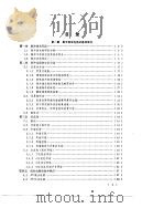
Chapter 1:Introduction1
1.1A Historical Perspective2
1.2 Issues in Digital Integrated Circuit Design4
1.3 To Probe Further12
1.4 Exercises15
PART Ⅰ:A CIRCUIT PERSPECTIVE17
Chapter 2:The Devices17
2.1Introduction18
2.2The Diode18
2.2.1 A First Glance at the Device19
2.2.2 Static Behavior22
2.2.3 Dynamic,or Transient,Behavior27
2.2.4 The Actual Diode—Secondary Effects36
2.2.5 The SPICE Diode Model38
2.3The MOS(FET)Transistor39
2.3.1 A First Glance at the Device39
2.3.2 Static Behavior41
2.3.3 Dynamic Behavior47
2.3.4 The Actual MOS Transistor—Secondary Effects50
2.3.5 SPICE Models for the MOS Transistor57
2.4The Bipolar Transistor62
2.4.1 A First Glance at the Device63
2.4.2 Static Behavior64
2.4.3 Dynamic Behavior72
2.4.4 The Actual Bipolar Transistor—Secondary Effects79
2.4.5 SPICE Models for the Bipolar Transistor81
2.5 A Word on Process Variations84
2.6 Perspective:Future Device Developments86
2.7 Summary87
2.8 To Probe Further89
2.9 Exercises and Design Problems90
Appendix A:Layout Design Rules97
Appendix B:Small-Signal Models105
Chapter 3:The Inverter108
3.1Introduction109
3.2Definitions and Properties109
3.2.1 Area and Complexity109
3.2.2 Functionality and Robostness:The Static Behavior110
3.2.3 Performance:The Dynamic Behavior116
3.2.4 Power and Energy Consumption119
3.3The Static CMOS Inverter120
3.3.1 A First Glance120
3.3.2 Evaluating the Robusmess of the CMOS Inverter:The Static Behavior124
3.3.3 Performance of CMOS Inverter:The Dynamic Behavior129
3.3.4 Power Consumption and Power-Delay Product141
3.3.5 A Look into the Future:Effects of Technology Scaling146
3.4The Bipolar ECL Inverter150
3.4.1 Issues in Bipolar Digital Design:A Case Study150
3.4.2 The Emitter-Coupled Logic(ECL)Gate at a Glance155
3.4.3 Robustness and Noise Immunity:The Steady-State Characteristics160
3.4.4 ECL Switching Speed:The Transient Behavior165
3.4.5 Power Consumption176
3.4.6 Looking Ahead:Scaling the Technology177
3.5 Perspective:Area,Performance,and Dissipation179
3.6 Summary179
3.7 To Probe Further180
3.8 Exercises and Design Problems181
Chapter 4:Designing Combinational Logic Gates in CMOS189
4.1Introduction190
4.2Static CMOS Design191
4.2.1 Complementary CMOS191
4.2.2 Ratioed Logic202
4.2.3 Pass-Transistor Logic210
4.3Dynamic CMOS Design222
4.3.1 Dynamic Logic:Basic Principles223
4.3.2 Performance of Dynamic Logic225
4.3.3 Noise Considerations in Dynamic Design227
4.3.4 Cascading Dynamic Gates231
4.4Power Consumption in CMOS Gates234
4.4.1 Switching Activity of a Logic Gate234
4.4.2 Glitching in Static CMOS Circuits240
4.4.3 Short-Circuit Currents in Static CMOS Circuits242
4.4.4 Analyzing Power Consumption Using SPICE244
4.4.5 Low-Power CMOS Design246
4.5 Perspective:How to Choose a Logic Style252
4.6 Summary253
4.7 To Probe Further254
4.8 Exercises and Design Problems255
Appendix C:Layout Techniques for Complex Gates264
Chapter 5:Very High Performance Digital Circuits269
5.1Introduction270
5.2Bipolar Gate Design270
5.2.1 Logic Design in ECL270
5.2.2 Differendal ECL272
5.2.3 Current Mode Logic278
5.2.4 ECL with Active Pull-Downs281
5.2.5 Altemative Bipolar Logic Styles283
5.3The BiCMOS Approach287
5.3.1 The BiCMOS Gate at a Glance288
5.3.2 The Static Behavior and Robusmess Issues291
5.3.3 Performance of the BiCMOS Inverter293
5.3.4 Power Consumption297
5.3.5 Technology Scaling298
5.3.6 Designing BiCMOS Digital Gates299
5.4Digital Gallium Arsenide Design300
5.4.1 GaAs Devices and Their Properties301
5.4.2 GaAs Digital Circuit Design307
5.5Low-Temperature Digital Circuits312
5.5.1 Low-Temperature Silicon Digital Circuits312
5.5.2 Superconducting Logic Circuits314
5.6 Perspective:When to Use High-Performance Technologies321
5.7 Summary322
5.8 To Probe Further323
5.9 Exercises and Design Problems325
Appendix D:The Schottky-Barrier Diode330
Chapter 6:Designing Sequential Logic Circuits332
6.1Introduction333
6.2Static Sequential Circuits333
6.2.1 Bistability333
6.2.2 Flip-Flop Classification335
6.2.3 Master-Slave and Edge-Triggered FFs338
6.2.4 CMOS Static Flip-Flops341
6.2.5 Bipolar Static Flip-Flops345
6.3Dynamic Sequential Circuits347
6.3.1 The Pseudostatic Latch348
6.3.2 The Dynamic Two-Phase Flip-Flop350
6.3.3 The C2MOS Latch351
6.3.4 NORA-CMOS—A Logic Style for Pipelined Structures355
6.3.5 True Single-Phase Clocked Logic (TSPCL)359
6.4Non-Bistable Sequential Circuits362
6.4.1 The Schmitt Trigger363
6.4.2 Monostable Sequential Circuits369
6.4.3 Astable Circuits371
6.5 Perspective:Choosing a Clocking Strategy374
6.6 Summary375
6.7 To Probe Further375
6.8 Exercises and Design Problems376
PART Ⅱ:A SYSTEMS PERSPECTIVE383
Chapter 7:Designing Arithmetic Building Blocks383
7.1Introduction384
7.2 Datapaths in Digital Processor Architectures384
7.3The Adder386
7.3.1 The Binary Adder:Definitions386
7.3.2 The Full Adder:Circuit Design Considerations389
7.3.3 The Binary Adder:Logic Design Considerations396
7.4The Multiplier408
7.4.1 The Multiplier:Definitions408
7.4.2 The Array Multiplier408
7.4.3 Other Multiplier Structures412
7.5The Shifter414
7.5.1 Barrel Shifter414
7.5.2 Logarithmic Shifter416
7.6 Other Arithmetic Operators417
7.7Power Considerations in Datapath Structures418
7.7.1 Reducing the Supply Voltage418
7.7.2 Reducing the Effective Capacitance421
7.8 Perspective:Design as a Trade-off424
7.9 Summary425
7.10 To Probe Further426
7.11 Exercises and Design Problems427
Appendix E:From Datapath Schematics to Layout434
Chapter 8:Coping with Interconnect438
8.1Introduction439
8.2Capacitive Parasitics439
8.2.1 Modeling Interconnect Capacitance439
8.2.2 Capacitance and Reliability—Cross Talk445
8.2.3 Capacitance and Performance in CMOS446
8.2.4 Capacitance and Performance in Bipolar Design461
8.3Resistive Parasitics464
8.3.1 Modeling and Scaling of Interconnect Resistance464
8.3.2 Resistance and Reliability—Ohmic Voltage Drop467
8.3.3 Electromigration469
8.3.4 Resistance and Performance—RC Delay471
8.4Inductive Parasitics477
8.4.1 Sources of Parasitic Inductances477
8.4.2 Inductance and Reliability—Voltage Drop478
8.4.3 Inductance and Performance—Transmission Line Effects482
8.5Comments on Packaging Technology493
8.5.1 Package Materials494
8.5.2 Interconnect Levels494
8.5.3 Thermal Considerations in Packaging499
8.6 Perspective:When to Consider Interconnect Parasitics500
8.7 Chapter Summary501
8.8 To Probe Further502
8.9 Exercises and Design Problems503
Chapter 9:Timing Issues in Digital Circuits510
9.1Introduction511
9.2Clock Skew and Sequential Circuit Performance511
9.2.1 Single-Phase Edge-Triggered Clocking513
9.2.2 Two-Phase Master-Slave Clocking515
9.2.3 Other Clocking Styles517
9.2.4 How to Counter Clock Skew Problems517
9.2.5 Case Study—The Digital Alpha 21164 Microprocessor520
9.3Self-Timed Circuit Design522
9.3.1 Self-Timed Concept522
9.3.2 Completion-Signal Generation525
9.3.3 Self-Timed Signaling528
9.4Synchronizers and Arbiters533
9.4.1 Synchronizers—Concept and Implementation533
9.4.2 Arbiters538
9.5Clock Generation and Synchronization538
9.5.1 Clock Generators538
9.5.2 Synchronization at the System Level540
9.6 Perspective:Synchronous versus Asynchronous Design543
9.7 Summary544
9.8 To Probe Further544
9.9 Exercises and Design Problems545
Chapter 10:Designing Memory and Array Structures551
10.1Introduction552
10.2Semiconductor Memories—An Introduction552
10.2.1 Memory Classification552
10.2.2 Memory Architectures and Building Blocks555
10.3The Memory Core559
10.3.1 Read-Only Memories559
10.3.2 Nonvolatile Read-Write Memories573
10.3.3 Read-Write Memories(RAM)578
10.4Memory Peripheral Circuitry590
10.4.1 The Address Decoders591
10.4.2 Sense Amplifiers596
10.4.3 Drivers/Buffers603
10.4.4 Timing and Control603
10.5Memory Reliability and Yield605
10.5.1 Signal-To-Noise Ratio605
10.5.2 Memory yield610
10.6Case Studies in Memory Design611
10.6.1 The Programmable Logic Array(PLA)612
10.6.2 A 4 Mbit SRAM616
10.7 Perspective:Semiconductor Memory Trends and Evolutions617
10.8 Summary620
10.9 To Probe Further621
10.10 Exercises and Design Problems622
Chapter 11:Design Methodologies629
11.1Introduction630
11.2Design Analysis and Simulation630
11.2.1 Representing Digital Data as a Continuous Entity631
11.2.2 Representing Data as a Discrete Entity633
11.2.3 Using Higher-Level Data Models637
11.3Design Verification638
11.3.1 Electrical Verification639
11.3.2 Timing Verification640
11.3.3 Functional(or Formal)Verification641
11.4Implementation Approaches642
11.4.1 Custom Circuit Design643
11.4.2 Cell-Based Design Methodology646
11.4.3 Array-Based Implementation Approaches655
11.5Design Synthesis667
11.5.1 Circuit Synthesis668
11.5.2 Logic Synthesis669
11.5.3 Architecture Synthesis671
11.6Validation and Testing of Manufactured Circuits672
11.6.1 Test Procedure674
11.6.2 Design for Testability675
11.6.3 Test-Pattern Generation684
11.7 Perspective and Summary687
11.8 To Probe Further688
11.9 Exercises and Design Problems691
Problem Solutions693
Index700
1999《数字集成电路 设计透视 英文 影印版》由于是年代较久的资料都绝版了,几乎不可能购买到实物。如果大家为了学习确实需要,可向博主求助其电子版PDF文件(由拉贝(Rabaey J.M.)著 1999 北京:清华大学出版社 出版的版本) 。对合法合规的求助,我会当即受理并将下载地址发送给你。
高度相关资料
-
- 数字逻辑电路分析与设计 英文版
- 1997 北京:清华大学出版社
-
- 数字集成电路 设计原理和应用
- 上海无线电十九厂

-

- 数字电路与罗辑设计 译文
- 1979
-
- 数字集成电路与逻辑设计
- 1986 哈尔滨:黑龙江科学技术出版社
-

- 工程流体力学泵与风机 第2版
- 1985 北京:水利电力出版社
-

- MOS数字集成电路
- 1981 长沙:湖南科学技术出版社
-
- 数字集成电路设计原理和运用
- 1979 北京:国防工业出版社
-

- 数字计数电路
- 1981 北京:人民邮电出版社
-
- 数字集成电路基础
- 1986 北京:高等教育出版社
-
- 接口技术
- 1999 沈阳:东北大学出版社
-

- 数字集成电路分析和设计
- 1989 北京:国防工业出版社
-
- 数字逻辑电路设计
- 1984 北京:高等教育出版社
-

- 数字电路的逻辑设计
- 1980 长沙:湖南科学技术出版社
-
- 数字电路设计与实用电路
- 1988 广州:华南理工大学出版社
提示:百度云已更名为百度网盘(百度盘),天翼云盘、微盘下载地址……暂未提供。➥ PDF文字可复制化或转WORD