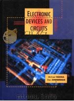
《ELECTRONIC DEVICES AND CIRCUITS》
| 作者 | 编者 |
|---|---|
| 出版 | PRENTICE HALL |
| 参考页数 | 1068 |
| 出版时间 | 没有确切时间的资料 目录预览 |
| ISBN号 | 无 — 求助条款 |
| PDF编号 | 819565848(仅供预览,未存储实际文件) |
| 求助格式 | 扫描PDF(若分多册发行,每次仅能受理1册) |
1 Introduction toElectronics2
1.1ELECTRONICS TODAY4
1.2 THE STUDY OF ELECTRONICS6
Multiple Small Exposures6
Study Techniques8
1.3 A WORD ABOUT CURRENT8
1.4 COMPUTER SIMULATION10
Sample Circuit Simulation Programs11
Using Computer Programs13
PART 1DIODES15
2The Ideal Diode16
2.1INTRODUCTION18
2.2 THE IDEAL DIODE19
2.3 DIODE-RESISTOR CIRCUITS20
Example 2.1 Simple Diode-Resistor Circuits22
Example 2.2 Single Loop Circuit23
Example 2.3 Multiple Resistor Circuit24
2.4 IS A DIODE ON OR OFF?—TWO APPROACHES25
Current Test26
Voltage Test26
Example 2.4 Diode Test27
2.5 CURRENT TRAFFIC CONTROL—DIODE LOGIC28
A Diode Logic Circuit28
2.6 AC TO DC CONVERSION—THE HALF-WAVE RECTIFIER30
Example 2.5 Half-Wave Rectifier Examples31
AC-DC Conversion32
Example 2.6 Finding DC Values33
2.7 AC TO DC CONVERSION—THE FULL-WAVE RECTIFIER34
The Diode Bridge Circuit34
2.8 DIODE LIMITERS (CLIPPERS)35
Top Clipping36
Example 2.7 Diode Limiters—Top Clipping38
Bottom Clipping38
Example 2.8 Diode Limiters—Bottom Clipping39
Symmetric Clipping39
Example 2.9 Symmetric Clipping Circuits40
3The Real Diode46
3.1INTRODUCTION48
3.2 DIODE CURRENT AND VOLTAGE(THE Ⅰ-Ⅴ CURVE)48
3.3 THE REAL DIODE51
The Improved Diode Model53
An Important Note53
Current Test53
Example 3.1 The Current Test Ⅰ54
Example 3.2 The Current Test Ⅱ54
Voltage Test55
Example 3.3 The Voltage Test55
3.4 DIODE CIRCUITS WITH REAL DIODES56
The Half-Wave Rectifier Circuit56
Example 3.4 The Half-Wave Rectifier57
The Full-Wave Rectifier59
Example 3.5 The Full-Wave Rectifier60
The Clipping Circuit61
Example 3.6 Two-Sided Limiting with Real Diodes61
3.5 DIODE RESISTANCE62
3.6 DIODE RATINGS—THE BREAKDOWN REGION64
The ON Diode64
Example 3.7 Approximating Power65
The Breakdown Region66
Example 3.8 Breakdown67
3.7 COMMERCIALLY AVAILABLE DIODES—THE DIODE DATA SHEET69
Catalog Data69
Example 3.9 Diode Selection69
Diode Data Sheets70
The Diode Reverse Current73
Reverse Recovery Time74
Example 3.10 Using the Data Sheet74
3.8 DIODE TESTING75
A Bad Diode (Using the VOM)75
A Bad Diode (Using the DMM)76
3.9 DIODE CIRCUIT TROUBLESHOOTING76
Example 3.11 Troubleshooting the Diode Limiter78
Multimeter Testing78
4Diode—ReactiveCircuits86
4.1 INTRODUCTION88
4.2 THE CAPACITOR AS BATTERY88
Example 4.1 Capacitor Discharge89
4.3 HALF-WAVE RECTIFIER WITH CAPACITOR90
Ripple90
Example 4.2 Half-Wave Rectifier with Capacitor Ⅰ92
Example 4.3 Half-Wave Rectifier with Capacitor Ⅱ93
rms Ripple Factor93
4.4 THE FULL-WAVE RECTIFIER WITH CAPACITOR94
Example 4.4 Full-Wave Rectifier with Capacitor95
Rectifier with Transformer95
Example 4.5 Bridge Rectifier with Transformer96
The Center-Tapped Transformer96
Example 4.6 Center-Tapped Transformer Rectifier97
4.5 DIODE CURRENT RATINGS97
Half-Wave Rectifier97
Example 4.7 Diode Currents98
Example 4.8 Determining the Diode On-Time99
Full-Wave Rectifiers99
Diode Current Ratings100
4.6 THE PEAK DETECTOR101
Example 4.9 Peak Detector101
4.7 THE DIODE AM DEMODULATOR102
Example 4.10 AM Demodulation104
4.8 DIODE CLAMPING CIRCUITS105
Example 4.11 Clamping Circuits107
4.9 THE VOLTAGE DOUBLER108
4.10 DIODE-INDUCTOR CIRCUIT (FLYBACK)109
Flyback Prevention111
4.11 TROUBLESHOOTING DIODE-CAPACITOR CIRCUITS112
The Capacitor112
Example 4.12 Troubleshooting112
Example 4.13 Troubleshooting Ⅱ113
5The Zener Diode—VoltageRegulation120
5.1 INTRODUCTION122
5.2 THE ZENER DIODE123
Zener Diode Basics123
The Real Zener Diode125
5.3 ZENER DIODE CIRCUITS126
Example 5.1 Zener Circuit127
Zener Diode-Resistor Load Circuit128
Is the Zener Diode in Breakdown?—An Alternate Approach129
Example 5.2 Zener Diode—Resistor Circuit Ⅰ129
Minimum Load Resistance130
Example 5.3 Zener Diode—Resistor Circuit Ⅱ130
5.4 ZENER CLIPPER CIRCUITS131
Example 5.4 Zener Clipper133
5.5 ZENER VOLTAGE REGULATOR CIRCUIT134
Example 5.5 Zener Regulator—Minimum Load135
Example 5.6 Zener Regulator—Regulator Resistor135
5.6 INTEGRATED CIRCUIT VOLTAGE REGULATORS136
5.7 TROUBLESHOOTING ZENER DIODES AND CIRCUITS137
Example 5.7 Troubleshooting a Zener Diode Circuit139
6Special-PurposeDiodes andOpto-Electrical Devices146
6.1 INTRODUCTION148
Specialized Diodes148
Troubleshooting Specialized Diodes148
6.2 THE GERMANIUM DIODE148
Example 6.1 The Germanium Diode149
6.3 THE SCHOTTKY DIODE150
Example 6.2 The Schottky Diode151
6.4 THE TUNNEL DIODE152
Example 6.3 The Tunnel Diode Circuit153
6.5 THE VARACTOR DIODE155
Example 6.4 The Varactor Diode156
6.6 THE PHOTO DIODE157
The Photoconductive Mode157
Example 6.5 The Photoconductive Cell158
The Light Spectrum159
Example 6.6 Frequency and Wavelength160
Commercial Photo Diodes Data Sheets161
The Photovoltaic Mode163
Example 6.7 The Photovoltaic Mode164
6.7 THE PHOTORESISTOR (PHOTOCONDUCTIVE CELL)165
Example 6.8 The Photoresistor167
6.8 LIGHT-EMITTING DIODES (LED)167
LED Basics167
Example 6.9 A Bad LED Design169
The Seven-Segment Display170
6.9 THE PHOTO TRANSISTOR AND OPTO-ISOLATOR172
The Photo Transistor172
The Opto-Isolator (Opto-Coupler)172
Fiber Optics174
PART 2 BIPOLAR UNCTION TRANSISTORS (BJT)179
7The NPN Bipolar Junction Transistor180
7.1 INTRODUCTION182
7.2 BJT STATES OF OPERATION183
Overview184
The Active State184
Example 7.1 Transistor Current Gain, β186
Example 7.2 Emitter Current-Collector Current Relations187
7.3 TRANSISTOR RATINGS188
Transistor Power188
Base Collector Breakdown (VCBO)189
7.4 SIMPLE DC TRANSISTOR CIRCUITS(IB CONTROL)189
Example 7.3 IB Control with Base Resistor192
Example 7.4 IB Control with Base Supply Voltage193
7.5 THE COLLECTOR RESISTOR196
Example 7.5 Collector Resistor197
7.6 THE CUT-OFF AND SATURATION STATES199
CUT-OFF199
SATURATION200
Example 7.6 Base Supply Voltage and Saturation Ⅰ202
Example 7.7 Base Supply Voltage and Saturation Ⅱ203
Example 7.8 Base Resistor and Saturation Ⅰ205
Example 7.9 Base Resistor and Saturation Ⅱ206
Example 7.10 Collector Resistor and Saturation Ⅰ207
Example 7.11 Collector Resistor and Saturation Ⅱ208
Example 7.12 Collector Supply Voltage and Saturation Ⅰ209
Example 7.13 Collector Supply Voltage and Saturation Ⅱ210
7.7 DETERMINING THE STATE OF A TRANSISTOR212
Example 7.14 Determining the State of a Transistor Ⅰ212
Example 7.15 Determining the State of a Transistor Ⅱ213
Example 7.16 Determining the State of a Transistor Ⅲ215
7.8 DC TRANSISTOR DATA SHEET216
8Troubleshooting222
8.1INTRODUCTION224
Temporary Breadboard Building224
Prototype Building224
Repairing a Circuit That Once Worked224
8.2 DC TROUBLESHOOTING, BRIEFLY225
Recording the Estimated and Measured Voltages226
Example 8.1 Recording Estimated Voltages227
Example 8.2 Recording the Measured Voltages228
8.3 THE COMPLETE DC TROUBLESHOOTING PROCEDURE229
Troubleshoot the Circuit229
Locate the Problem230
Example 8.3 DC Troubleshooting Ⅰ230
Example 8.4 DC Troubleshooting Ⅱ231
Example 8.5 DC Troubleshooting Ⅲ232
Example 8.6 DC Troubleshooting Ⅳ232
Example 8.7 DC Troubleshooting Ⅴ233
Summary of Examples234
8.4 TYPES OF COMPONENT FAILURES235
Resistor Failures235
Transistor Failures235
Open Circuit Failures in Transistors236
Short Circuit Failures in Transistors236
8.5 THE UNIVERSAL TRANSISTOR TEST CIRCUIT (UTTC)237
Determining if a Transistor Is Good or Bad with the UTTC238
Finding β3 with the UTTC239
8.6 DC TROUBLESHOOTING EXAMPLES239
Example 8.8 DC Troubleshooting Ⅵ239
Example 8.9 DC Troubleshooting Ⅶ240
Example 8.10 DC Troubleshooting Ⅷ241
Example 8.11 DC Troubleshooting Ⅸ241
Example 8.12 DC Troubleshooting Ⅹ242
8.7 TROUBLESHOOTING IN THE LABORATORY244
Why Not Current Measurements?245
Tips on Using the Temporary Breadboard in the Lab246
Common Problems in Using the Temporary Breadboards247
8.8 DC TROUBLESHOOTING ON THE JOB249
Obtaining the Circuit Diagram249
Making Enough Copies of the Circuit Diagram250
9Biasing for Linear Applications256
9.1 INTRODUCTION258
9.2 BASE VOLTAGE BIASING (VB CONTROL)259
Example 9.1 VB Control262
9.3 THE COLLECTOR RESISTOR263
Example 9.2 VB Control with Collector Resistor264
Example 9.3 Comparison of IB and VB Control266
Example 9.4 VB Control, Rc Variations267
Example 9.5 Variable Base Voltage Biasing269
9.4 THE VOLTAGE DIVIDER270
Example 9.6 The Voltage Divider271
Example 9.7 Approximate Voltage Divider with Load272
9.5 SELF-BIASING THE TRANSISTOR274
Example 9.8 Self-Biasing Circuit275
9.6 VOLTAGE AMPLIFICATION278
Example 9.9 Voltage Amplification280
Example 9.10 Eect of Rcon Voltage Amplification282
9.7 EXACT BASE VOLTAGE CALCULATIONS284
The Thevenin Approach284
Example 9.11 Thevenin Equivalent Ⅰ286
Example 9.12 Thevenin Equivalent Ⅱ287
Voltage Divider Versus the Exact Thevenin Approach288
9.8 DC TROUBLESHOOTING289
Voltage Divider Problems289
VB-Control Transistor Problems290
Transistor Failures292
Example 9.13 DC Troubleshooting294
10 The Common-Emitter Amplifier304
10.1INTRODUCTION306
Example 10.1 DC and AC Signal Components307
10.2 DC BIAS LEVELS308
Biasing308
Example 10.2 Bias Level Determination310
DC Bias and Output Voltage Limits311
Example 10.3 Maximum Voltage Swing Ⅰ313
Example 10.4 Maximum Voltage Swing Ⅱ314
10.3 THE AC BEHAVIOR OF THE TRANSISTOR315
Example 10.5 Small-Signal AC Emitter Resistor318
10.4 THE COMMON-EMITTER AMPLIFIER319
Example 10.6 The Common-Emitter Amplifier Ⅰ321
Example 10.7 The Common-Emitter Amplifier Ⅱ322
10.5 THE EMITTER BYPASS CAPACITOR323
The Capacitor323
The Emitter Bypass Capacitor324
Example 10.8 The Emitter Bypass Capacitor326
10.6 INPUT CAPACITOR COUPLING—THE SELF-BIASED CIRCUIT327
Example 10.9 The Input Coupling Capacitor329
10.7 THE LOAD RESISTOR330
Example 10.10 The Load Resistor333
10.8 TROUBLESHOOTING334
Example 10.11 Troubleshooting Ⅰ336
Example 10.12 Troubleshooting Ⅱ337
Example 10.13 Troubleshooting Ⅲ338
Example 10.14 Troubleshooting Ⅳ339
Example 10.15 Troubleshooting Ⅴ340
11The Box Model348
11.1 INTRODUCTION350
11.2 THE Box MODEL351
The Load Resistor352
Example 11.1 The Load Resistor Ⅰ352
Example 11.2 The Load Resistor Ⅱ354
Load Power355
The Source Resistor355
Example 11.3 The Source Resistance Ⅰ356
Example 11.4 The Source Resistance Ⅱ357
The Complete System358
Example 11.5 The Total System359
11.3 THE COMMON-EMITTER AMPLIFIER360
No-Load Gain361
Output Resistance362
Input Resistance363
General Derivation of Rbase363
Formal Derivation of Rbase364
Example 11.6 Box Model of the Common-Emitter Amplifier366
Example 11.7 Box Model of the Bypassed Common-EmitterAmplifier367
11.4 COMMON-EMITTER AMPLIFIER WITH LOAD AND SOURCE RESISTORS369
Load Resistor369
Example 11.8 Load Resistor370
Source Resistor372
Example 11.9 Source Resistor372
The Complete Common-Emitter Amplifier374
Example 11.10 The Complete Amplifier375
11.5 MULTISTAGE AMPLIFIER376
Example 11.11 Two-Stage Amplifier379
12The Emitter Follower (TheCommon-CollectorAmplifier)388
12.1 INTRODUCTION—THE BUFFER AMPLIFIER390
Example 12.1 The Buffer392
Example 12.2 Buffer Design393
12.2 THE EMITTER FOLLOWER COMMON-COLLECTOR AMPLIFIER)395
No-Load Gain395
Example 12.3 Emitter-Follower Box Model Gain396
Input Resistance398
Example 12.4 Emitter Follower Input Resistance399
Output Resistance400
Example 12.5 Emitter-Follower Output Resistance402
The Complete Box Model403
Example 12.6 The Complete Emitter Follower404
12.3 THE EMITTER FOLLOWER AS A CURRENT BUFFER406
Example 12.7 The Current Buffer407
12.4 ZENER VOLTAGE REGULATION AND THE CURRENT BUFFER408
Example 12.8 Zener Regulation409
12.5 TROUBLESHOOTING411
Shorted CL411
Open CL412
13Improved BJT AC Models418
13.1 INTRODUCTION420
13.2 BJT TRANSISTOR CHARACTERISTIC CURVES420
13.3 THE SIMPLE BJT MODEL423
Example 13.1 The Simple BJT AC Model424
13.4 THE HYBRID-PI BJT MODEL425
The Hybrid-Pi Model425
Example 13.2 The Early Voltage and ro427
Example 13.3 The Hybrid-Pi Model427
Example 13.4 The Hybrid-Pi Model with ro428
Alternate Hybrid-Pi Model429
13.5 THE H-PARAMETER BJT MODEL430
Example 13.5 h-Parameter Model431
Example 13.6 The BJT h-Parameter Model432
13.6 MODEL COMPARISONS433
Simple Model <—> Hybrid-Pi Model433
Hybrid-Pi Model <—> h-Parameter Model434
13.7 BJT DATA SHEETS435
Interpreting Data Sheets435
Determining the Early Voltage435
14The PNP Transistor442
14.1 INTRODUCTION444
14.2 VB CONTROL OF PNP TRANSISTORS446
Example 14.1 VB Control Ⅰ449
Example 14.2 VB Control Ⅱ450
14.3 DOUBLE-SIDED SUPPLY BIASING451
Example 14.3 Double-Sided Supply Voltages452
14.4 THE PNP COMMON-EMITTER AMPLIFIER453
DC Bias Analysis453
AC Analysis—The Box Model454
Gain455
Input Resistance455
Output Resistance455
System Gain456
Example 14.4 The PNP Common-Emitter Amplifier456
14.5 THE PNP EMITTER FOLLOWER COMMON-COLLECTOR)458
DC Bias Analysis458
AC Analysis—The Box Model458
Gain459
Input Resistance459
Output Resistance460
System Gain460
Example 14.5 The PNP Emitter Follower460
14.6 IB CONTROL462
Example 14.6 Comparison of the NPN and PNP Inverters463
14.7 COMBINED NPN-PNP CIRCUITS465
VB Control465
IB Control466
Current Gain467
14.8 TROUBLESHOOTING468
Bad Connections468
Transistor Open Failures469
Transistor Short Failures469
AC Signal Tracing470
Example 14.7 Troubleshooting470
15The Common-Base Amplifier480
15.1 INTRODUCTION482
15.2 DC BIASING OF THE COMMON-BASE AMPLIFIER482
The NPN Common-Base Amplifier482
The PNP Common-Base Amplifier484
Example 15.1 DC Bias Levels in the Common-Base Amplifier485
15.3 AC BEHAVIOR OF THE COMMON-BASE AMPLIFIER—BOX MODEL486
Gain487
Output Resistance488
Input Resistance488
Example 15.2 Box Model of the Common-Base Amplifier489
15.4 THE COMPLETE COMMON-BASE AMPLIFIER490
Example 15.3 Complete AC Analysis of the Common-Base Amplifier491
15.5 AMPLIFIER COMPARISONS492
15.6 TROUBLESHOOTING492
Example 15.4 DC Troubleshooting the Common-Base493
Example 15.5 AC Signal Tracing in the Common-Base Amplifier494
16Specialized Transistor Circuits500
16.1 INTRODUCTION502
16.2 THE DARLINGTON CONNECTION502
Equivalent AC Emitter Resistance503
16.3 DARLINGTON COMMON-EMITTER AMPLIFIER504
DC Bias Levels504
AC Analysis—the Box Model505
Example 16.1 The Darlington Common-Emitter Amplifier506
16.4 THE CASCODE AMPLIFIER508
DC Analysis508
Example 16.2 DC Analysis of the Common-Base Amplifier510
16.5 THE CASCODE AMPLIFIER—AC ANALYSIS512
Example 16.3 Cascode Amplifier—AC Analysis514
16.6 COLLECTOR-FEEDBACK BIASING515
Example 16.4 Collector-Feedback Biasing516
16.7 ANALYSIS OF COLLECTOR-FEEDBACK BIASING—THE MILLER EFFECT517
Input Resistance—The Miller Effect518
Example 16.5 Collector Feedback—AC Analysis520
17The Differential Amplifier526
17.1 INTRODUCTION528
17.2 BIASING THE DIFFERENTIAL AMPLIFIER530
Example 17.1 NPN Differential Amplifier Biasing531
Example 17.2 Current Source Biasing533
Example 17.3 PNP Differential Amplifier Biasing533
17.3 THE DIFFERENTIAL MODE535
Example 17.4 Differential-Mode Gain538
The Differential-Mode Box Model539
Limits on Input Voltage Difference540
17.4 COMMON-MODE GAIN541
Example 17.5 Common-Mode Gain544
17.5 THE GENERAL DIFFERENTIAL AMPLIFIER545
Example 17.6 General Differential Amplifier Response546
17.6 INTEGRATED CIRCUIT DIFFERENTIAL AMPLIFIERS548
Example 17.7 Instrumentation Amplifiers551
17.7 TROUBLESHOOTING552
Open Failures552
Short Failures553
Example 17.8 Troubleshooting Differential Amplifier Circuits554
Troubleshooting Integrated Circuit Amplifiers554
18Current Sources562
18.1 INTRODUCTION564
18.2 THE BASIC NPN TRANSISTOR CURRENT SOURCE565
VB Control565
Example 18.1 The NPN Current Source566
Maximum Load Voltage and Resistance567
Example 18.2 Maximum Load Voltage and Current568
18.3 THE BASIC PNP TRANSISTOR CURRENT SOURCE568
VB Control569
Maximum Load Voltage and Resistance569
Example 18.3 The PNP Current Source570
18.4 NEGATIVE VOLTAGE SUPPLY CURRENT SOURCES571
NPN571
Example 18.4 Negative Voltage Supply NPN Current Source572
PNP573
Example 18.5 Negative Voltage Supply PNP Current Source573
18.5 TEMPERATURE COMPENSATION575
Example 18.6 Temperature Compensation576
18.6 THE CURRENT MIRROR578
Example 18.7 Negative Supply NPN Current Mirror580
Example 18.8 PNP Current Mirror580
18.7 CURRENT SOURCE BIASING OF DIFFERENTIAL AMPLIFIERS581
DC Bias582
Box Model582
Common-Mode Rejection Ratio583
Current Source Output Resistance583
Example 18.9 Differential Amplifier583
19Power Amplifiers590
19.1 INTRODUCTION592
19.2 THE COMMON-EMITTER AMPLIFIER—MAXIMUM VOLTAGE SWING593
Symmetrical Swing594
Example 19.1 Maximum Symmetrical Swing595
Example 19.2 Maximum Swing—Common-Emitter Amplifier597
Capacitor Coupling and the Bypass Capacitor598
Example 19.3 Common Emitter with Capacitors Ⅰ599
Example 19.4 Common Emitter with Capacitors Ⅱ599
19.3 THE EMITTER FOLLOWER—MAXIMUM VOLTAGE SWING601
Example 19.5 Emitter Follower—Maximum Swing601
19.4 CLASS A POWER CONSIDERATIONS603
Example 19.6 Power Calculations for the Class A Amplifier605
19.5 TRANSFORMER COUPLING607
Analysis of the Transformer-Coupled Amplifier608
Power Calculations610
Example 19.7 Transformer-Coupled Class A Amplifier611
19.6 THE CLASS B AMPLIFIER612
Operation612
Power Considerations614
Example 19.8 Class B Maximum Power Calculations616
Example 19.9 Class B Power Calculations617
Distortion in the Class B Amplifier618
19.7 PUSH-PULL AMPLIFIER BIASING619
Example 19.10 Class B Biasing620
Diode Biasing621
Single-Supply Biasing622
Example 19.11 Single-Supply Diode Biasing622
The Bridge Amplifier and Phase Splitter623
19.8 TROUBLESHOOTING624
Short Circuit Failures625
Example 19.12 Q2 Short Failures626
Open Circuit Failures626
PART 3 FIELD EFFECT TRANSISTORS (FET)637
20The Field Effect Transistor638
20.1 INTRODUCTION640
20.2 THE JUNCTION FIELD EFFECT TRANSISTOR (JFET)641
JFET Operating States644
Example 20.1 Determining the Pinch-Off Voltage644
BJT SATURATION Region—JFET OHMIC Region645
Example 20.2 The OHMIC Region646
20.3 ACTIVE REGION DRAIN CURRENT VS.GATE VOLTAGE (ID-VGS)647
The ID-VGs Curve647
Example 20.3 Constructing the ID-VGS Curve648
The CUT-OFF, PINCH-OFF Confusion649
20.4 BASIC N-CHANNEL JFET BIASING650
Example 20.4 N-Channel JFET Biasing651
Example 20.5 The OHMIC Region652
20.5 SINGLE-SOURCE JFET BIASING (GRAPHICAL)653
Determining the Q-Point653
Example 20.6 Graphical Bias Calculations655
But I Can’t Find the JFET Ⅰ-Ⅴ Curve!656
Example 20.7 Constructing the JFET Ⅰ-V Curve657
20.6 SINGLE-SOURCE JFET BIASING (ANALYTICAL)657
Example 20.8 Analytical Bias Calculation658
20.7 VOLTAGE DIVIDER BIASING659
Example 20.9 Voltage Divider Biasing661
Analytical Calculation of Bias Levels661
Example 20.10 Voltage Divider Biasing—Analytical Calculation662
The Universal JFET Ⅰ-V Curve662
20.8 THE P-CHANNEL JFET663
Finding Bias Values663
Example 20.11 P-Channel Biasing (VG = OV)664
Example 20.12 Voltage Divider P-Channel Biasing665
Analytical Calculations667
Example 20.13 Analytical Bias Calculation (VG = OV)667
Example 20.14 Voltage Divider Biasing—Analytical668
20.9 JFET DATA SHEETS AND COMPUTER MODELS668
JFET Specifications670
JFET Computer Model670
Example 20.15 Data Sheet Parameters and Computer Model Parameters671
20.10 TROUBLESHOOTING THE JFET672
Out-of-Circuit Tests672
DC Troubleshooting of JFET Circuits673
Example 20.16 DC Troubleshooting674
21The MOSFET682
21.1 INTRODUCTION684
21.2 THE N-CHANNEL D-MOSFET684
Structure and Function684
Example 21.1 Biasing the D-MOSFET, Depletion Region686
Example 21.2 Biasing the D-MOSFET, Enhancement Region687
Example 21.3 D-MOSFET Biasing, Analytical Method688
The Almost Universal N-Channel D-MOSFET Ⅰ-V Curve688
21.3 THE P-CHANNEL D-MOSFET689
Structure and Function689
Example 21.4 Biasing the P-Channel D-MOSFET690
Example 21.5 P-Channel D-MOSFET Biasing, AnalyticalMethod691
The Almost Universal P-Channel D-MOSFET Ⅰ-V Curve692
21.4 THE N-CHANNEL E-MOSFET692
Structure and Function692
Example 21.6 N-Channel E-MOSFET Biasing693
Analytical N-Channel E-MOSFET Biasing694
Example 21.7 N-Channel E-MOSFET Biasing, Analytical Method695
The Almost-Universal N-Channel E-MOSFET Ⅰ-V Curve695
21.5 THE P-CHANNEL E-MOSFET696
Structure and Function696
Example 21.8 P-Channel E-MOSFET Biasing696
Analytical P-Channel E-MOSFET Biasing697
Example 21.9 P-Channel E-MOSFET Biasing, Analytical Method698
The Almost Universal P-Channel E-MOSFET Ⅰ-V Curve698
21.6 MOSFET DATA SHEETS AND COMPUTER MODELS699
Data Sheets699
21.7 THE COMPLEMENTARY MOSFET (CMOS)—AN INVERTER703
21.8 OTHER MOSFETs704
Power FETs705
Dual-Gate MOSFETs705
The MESFET705
21.9 DC TROUBLESHOOTING MOSFET CIRCUITS705
DC Troubleshooting the D-MOSFET705
Open Failures706
Short Failures707
DC Troubleshooting the E-MOSFET707
22FET AC Behavior and Applications716
22.1INTRODUCTION718
22.2 FET AC MODEL718
Determining gm for the JFET and D-MOSFET719
Example 22.1 Finding gm for the JFET720
Determining gm for the E-MOSFET720
Example 22.2 Finding gm for the E-MOSFET721
FET Data Sheets and AC Parameters721
FET OHMIC Region Resistance724
22.3 THE COMMON-SOURCE FET AMPLIFIER725
Common Source Box Model Parameters725
Example 22.3 The Common-Source Amplifier726
22.4 ADDITIONAL FET CIRCUITS728
Example 22.4 The FET Follower729
22.5 FET-BJT CIRCUITS731
22.6 THE VOLTAGE VARIABLE RESISTOR732
Resistance of FET733
Example 22.5 The FET as a Voltage Variable Resistor733
Automatic Gain Control (AGC)734
22.7 CMOS LOGIC CIRCUITS735
Inverter735
NAND Gate736
NOR Gate737
Special Topic FET Modeling739
BJT Models739
FET Models740
PART 4 THE OPERATIONAL AMPLIFIERS745
23 The Operational Amplifier(OP-AMP)746
23.1 INTRODUCTION748
23.2 THE OPERATIONAL AMPLIFIER (OP-AMP)748
23.3 NEGATIVE FEEDBACK750
Talking Around the Loop751
The General Negative Feedback Amplifier753
Example 23.1 Closed-Loop Gain754
High Forward Gain755
23.4 THE NON-INVERTING AMPLIFIER—TALKING AROUND THE LOOP756
The Unity-Gain Amplifier (Buffer Amplifier)756
Example 23.2 The Unity-Gain (Buffer) Amplifier757
The Non-Inverting Amplifier758
Example 23.3 The Non-Inverting Amplifier759
Example 23.4 Non-Inverting Amplifier Design760
23.5 THE INVERTING AMPLIFIER—TALKING AROUND THE LOOP760
Example 23.5 The Inverting Amplifier762
Example 23.6 The Inverting Amplifier, Design762
23.6 THE IDEAL OP-AMP763
Non-Inverting Amplifier764
Example 23.7 The Non-Inverting Amplifier765
Inverting Amplifier766
Example 23.8 The Inverting Op-Amp Amplifier767
23.7 THE REAL OP-AMP768
Input Bias Current769
Example 23.9 The Non-Inverting Amplifier770
Input Offset Voltage771
Bandwidth (Gain-Bandwidth Product)771
Example 23.10 Bandwidth and Gain-Bandwidth Product772
Rise Time and Slew Rate772
Op-Amp Data Sheets773
23.8 INSTRUMENTATION AMPLIFIERS776
23.9 TROUBLESHOOTING OP-AMP CIRCUITS778
Example 23.11 Op-Amp Troubleshooting778
24Operational Amplifier Circuits788
24.1 INTRODUCTION790
Non-Inverting Amplifier790
Unity-Gain Buffer Amplifier790
Inverting Amplifier791
Op-Amp Analysis Procedure792
Troubleshooting792
24.2 SUMMING AMPLIFIERS792
Inverting Summer792
Example 24.1 The Inverting Summer794
Example 24.2 Digital-to-Analog Converter (DAC)795
Inverting Amplifier with Buffers796
Non-Inverting Summer796
Example 24.3 Non-Inverting Amplifier797
Example 24.4 Non-Inverting Summing Amplifier798
Troubleshooting799
24.3 DIFFERENCE (DIFFERENTIAL) AMPLIFIER800
Differential Amplifier801
The Bridge Amplifier802
Example 24.5 Bridge Amplifier802
Troubleshooting803
24.4 DIFFERENTIATION AND INTEGRATION804
Differentiation804
A Note of Caution806
Example 24.6 Differentiation806
25Non-Linear Operational Amplifier Circuits802
Integration807
Example 24.7 Op-Amp Integration808
Troubleshooting809
24.5 IMPROVED VOLTAGE REGULATION809
Example 24.8 Buffered Zener with Voltage Divider810
Troubleshooting811
25.1 INTRODUCTION822
25.2 RECTIFIERS823
Simple Inverting Rectifier823
Example 25.1 Simple Inverting Rectifier824
Precision Rectifiers824
Non-Inverting Precision Rectifier824
Example 25.2 Non-Inverting Rectifier825
Inverting Precision Rectifier826
Example 25.3 Inverting Precision Rectifier827
Troubleshooting828
25.3 LIMITERS829
Op-Amp Limiter Circuit829
Example 25.4 Op-Amp Limiter830
Troubleshooting830
25.4 ZERO-CROSSING DETECTOR831
Example 25.5 Zero-Crossing Detector833
25.5 COMPARATORS LEVEL DETECTORS)833
The Non-Inverting Comparator834
Example 25.6 Non-Inverting Comparator834
Voltage Divider Reference Voltage for Comparator835
The Inverting Comparator835
Example 25.7 Voltage Level Indicator835
Troubleshooting837
25.6 SCHMITT TRIGGER837
Positive Feedback837
Example 25.8 The Schmitt Trigger839
Troubleshooting841
PART 5ADVANCED TOPICS RESPONSE AND FILTERS849
26Frequency Response850
26.1 INTRODUCTION852
26.2 THE GAIN RESPONSE853
Amplifier Gain853
Bandwidth853
Example 26.1 Half-Power Frequencies—Band-Pass Response855
Example 26.2 Half-Power Frequency—Low-Pass Response855
Example 26.3 Half-Power Frequency—High-Pass Response856
26.3 THE BODE GAIN PLOT857
Example 26.4 Log f Scale—Decades858
Example 26.5 Log f Scale—Octaves858
Example 26.6 3-dB Frequencies—Band-Pass Response860
Example 26.7 3-dB Frequency—Low-Pass Response861
Example 26.8 3-dB Frequency—High-Pass Response861
26.4 LOW-FREQUENCY RESPONSE—COUPLING CAPACITORS862
Capacitor Reactance863
The 3-dB Frequency864
Example 26.9 Simple RC Circuit864
Two-Resistor Circuit865
Example 26.10 Two-Resistor, Single Capacitor Circuit865
The Box Model866
Example 26.11 Common-Emitter Amplifier867
Example 26.12 Common-Source Amplifier868
Op-Amp Amplifiers870
Example 26.13 Inverting Op-Amp AC Amplifier870
Example 26.14 Non-Inverting Op-Amp AC Amplifier871
26.5 LOW-FREQUENCY RESPONSE—BYPASS CAPACITORS872
Example 26.15 Source Bypass Capacitor874
26.6 HIGH-FREQUENCY RESPONSE—THE MILLER EFFECT875
Amplifiers with Bypass Capacitors876
The Miller Capacitance877
Example 26.16 Complete Common-Emitter Frequency Response879
Example 26.17 Complete Common-Source Frequency Response880
Amplifiers without Bypass Capacitors882
26.7 MULTISTAGE AMPLIFIERS883
Common Emitter-to-Common Emitter (CE-CE)883
Emitter Follower-to-Common Emitter (EF-CE)883
Cascode Amplifier (Common Base-to-Common Emitter)885
26.8 TRANSISTOR DATA SHEETS886
BJT Data Sheet886
Example 26.18 BJT High-Frequency Parameters888
JFET Data Sheet888
26.9 OP-AMP FREQUENCY RESPONSE890
The Gain-Bandwidth Product891
27Active Filters898
27.1 INTRODUCTION900
27.2 Low-PASS FILTERS901
The Ideal Low-Pass Filter901
The Passive First-Order Low-Pass Filter902
Example 27.1 First-Order Passive RC Filter903
27.3 THE Low-PAss ACTIVE FILTER904
First-Order Filters904
Example 27.2 First-Order Low-Pass Active Filter905
Second-Order Filters906
Example 27.3 Sallen-Key Filter907
27.4 THE HIGH-PASS ACTIVE FILTER908
First-Order Filters909
Example 27.4 First-Order High-Pass Active Filter910
Second-Order Filters911
Example 27.5 Sallen-Key High-Pass Filter912
27.5 THE BAND-PASS ACTIVE FILTER913
Relating fL and fH to BW and fo914
High Pass-Low Pass Combination915
Example 27.6 High Pass-Low Pass Combination916
Sallen-Key Band-Pass Filter917
Example 27.7 Sallen-Key Band-Pass Filter919
27.6 HIGHER ORDER FILTERS920
27.7 TROUBLESHOOTING ACTIVE FILTERS921
Low-Pass Active Filter921
High-Pass Active Filter922
Band-Pass Active Filter923
Example 27.8 Troubleshooting the Low-Pass Filter923
28Feedback Amplifiers932
28.1 INTRODUCTION934
28.2 NEGATIVE FEEDBACK BASICS934
Terms and Formulas935
Example 28.1 Closed-Loop Gain935
Amplifier Parameter Variations and Non-Linearities936
28.3 POSITIVE FEEDBACK BASICS937
Stable Response938
Sustained Pulse939
Unstable Response940
Example 28.2 Positive Feedback940
28.4 STABILITY OF NEGATIVE FEEDBACK AMPLIFIERS941
Example 28.3 Phase Angle and Time Delay942
28.5 VOLTAGE FEEDBACK945
Four Feedback Possibilities945
Example 28.4 Feedback Analysis of Non-Inverting Amplifier946
BJT Feedback Analysis947
Example 28.5 BJT Voltage Out-Voltage Feedback Amplifier948
28.6 VOLTAGE OUT-CURRENT FEEDBACK948
Example 28.6 Voltage Out-Current Feedback Amplifier951
28.7 INPUT AND OUTPUT RESISTANCE—VOLTAGE FEEDBACK952
System Gain952
Input Resistance953
Output Resistance954
Example 28.7 Input and Output Resistance—Voltage Feedback954
28.8 INPUT AND OUTPUT RESISTANCE—CURRENT FEEDBACK955
System Gain955
Input Resistance956
Output Resistance957
Example 28.8 Input and Output Resistance—Current Feedback957
How Do I Know if a Transistor Amplifier Is Voltage or Current Feedback?958
28.9 CURRENT-OUT FEEDBACK AMPLIFIERS958
Current Out-Current Feedback Amplifier959
Current Out-Voltage Feedback Amplifier960
28.10 TROUBLESHOOTING961
Loosing the Feedback Loop (RF Fails Open)961
Degradation in the Forward-Path Amplifier962
A Note of Caution963
29Signal Generators972
29.1 INTRODUCTION974
29.2 THE CLASS C TUNED AMPLIFIER974
Example 29.1 The LC Tuned Circuit976
Example 29.2 Designing the LC Tuned Circuit976
The Class C Tuned Amplifier977
29.3 LC OSCILLATORS979
The Colpitts Oscillator979
Example 29.3 The Colpitts Oscillator980
Example 29.4 Colpitts Design981
The Hartley Oscillator982
Example 29.5 The Hartley Oscillator982
Example 29.6 Hartley Design983
Crystal Oscillator984
Variable Frequency Oscillators984
29.4 RC OSCILLATORS985
The RC Phase Shift Oscillator986
Example 29.7 The RC Phase Shift Oscillator987
The Wien Bridge Oscillator987
Example 29.8 The Wien Bridge Oscillator989
29.5 SQUARE WAVE GENERATOR989
Example 29.9 Pulse Wave Parameters990
Example 29.10 Square Wave Generator993
Example 29.11 Designing a Square Wave Generator993
29.6 TRIANGLE WAVE GENERATOR994
Example 29.12 Ramp Generator994
Example 29.13 Triangle Wave Generator995
Triangle Wave Generator996
The Sawtooth Generator996
29.7 INTEGRATED CIRCUIT SIGNAL GENERATORS997
The 555 Pulse Generator997
Example 29.14 The 555 Astable Multivibrator998
Function Generator Integrated Circuit998
29.8 TROUBLESHOOTING OSCILLATORS1000
Example 29.15 Troubleshooting LC Oscillators1000
Example 29.16 Troubleshooting RC Phase Shift Oscillators1001
30ElectronicSwitches(Thyristors)1008
30.1 INTRODUCTION1010
30.2 THE FOUR-LAYER DIODE AND THE DIAC1011
The Four-Layer Diode1011
Example 30.1 The Four-Layer Diode Relaxation Oscillator1013
The DIAC1013
30.3 THE SILICON-CONTROLLED RECTIFIER (SCR)1014
Turning the SCR OFF1016
Example 30.2 SCR Indicator Circuit1016
Example 30.3 SCR Relaxation Oscillator1017
False Triggering1017
Example 30.4 Four-Layer Diode Triggering of SCR1018
30.4 AC SCR APPLICATIONS1019
DC Motor Control1019
Example 30.5 Conduction Angle and DC Value1020
Example 30.6 SCR with Four-Layer Diode1021
RC Time-Delay Circuit1023
Example 30.7 RC Triggering Circuit1024
30.5 THE TRIAC1025
30.6 THE UNIJUNCTION TRANSISTOR (UJT)1027
UJT Basics1027
Example 30.8 UJT Vp Determination1029
Example 30.9 UJT Relaxation Oscillator1031
The Programmable Unijunction Transistor (PUT)1031
30.7 ADDITIONAL THYRISTORS1032
The Gate Turn-Off Switch (GTO)1033
The Silicon Bilateral Switch (SBS)1033
The Silicon-Controlled Switch (SCS)1033
Thyristor Optoisolators1034
《ELECTRONIC DEVICES AND CIRCUITS》由于是年代较久的资料都绝版了,几乎不可能购买到实物。如果大家为了学习确实需要,可向博主求助其电子版PDF文件(由 PRENTICE HALL 出版的版本) 。对合法合规的求助,我会当即受理并将下载地址发送给你。
高度相关资料
-

- Decision Support and Exoert Systems:Management Support Systems Third Edition
- 1993 Macmillan Publishing Company
-

- Electronic Devices and Circuit Alaysis
- 1986 DELMAR PUBLISHERS INC
提示:百度云已更名为百度网盘(百度盘),天翼云盘、微盘下载地址……暂未提供。➥ PDF文字可复制化或转WORD


