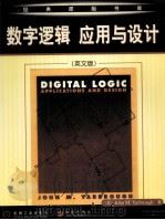
《DIGITAL LOGIC APPLICATIONS AND DESIGN》
| 作者 | JOHN M.YARBROUGH 编者 |
|---|---|
| 出版 | 未查询到或未知 |
| 参考页数 | 698 |
| 出版时间 | 没有确切时间的资料 目录预览 |
| ISBN号 | 711110837X — 求助条款 |
| PDF编号 | 812399288(仅供预览,未存储实际文件) |
| 求助格式 | 扫描PDF(若分多册发行,每次仅能受理1册) |
CHAPTER 1Digital Concepts and Number Systems1
Introduction1
1.1 Digital and Analog: Basic Concepts1
1.2 Some History of Digital Systems4
1.3 Impact of Digital Technology on Sociery6
1.4 Defining the Problem, an Introduction to Algorithms7
1.5 Digital Systems Overview9
1.6 Introduction to Number Systems9
1.7Positional Number Systems10
1.7.1 Decimal Numbers10
1.7.2 Binary Numbers11
1.7.3 Octal Numbers12
1.7.4 Hexadecimal Numbers12
1.7.5 Counting in Base r13
1.8Number System Conversion14
1.8.1 Binary to Hexadecimal Conversion15
1.8.2 Hexadecimal and Octal to Binary Conversion16
1.8.3 Binary to Decimal Conversion16
1.8.4 Successive Division Radix Conversion17
1.8.5 Fractional Radix Conversion, Successive Multiplication18
1.8.6 Radix Conversion Algorithm20
1.8.7 Decimal to Any Radix21
1.8.8 Any Radix to Decimal23
1.9 Binary Codes23
1.9.1Natural Binary Coded Decimal23
1.9.2 Binary Codes (Weighted)24
1.9.3 BCD Self-Complementing Codes25
1.9.4 Unit Distance Code26
1.9.5 Alphanumeric Codes28
1.9.6 Signed Number Binary Codes28
1.9.7 Signed Magnitude Codes28
1.9.8 Complement Codes29
1.10 Arithmetic32
1.10.1 Binary Arithmetic32
1.10.2 Binary Arithmetic Using Complement Codes35
1.10.3 Hexadecimal Arithmetic38
Summary42
References43
Glossary44
Questions and Problems45
CHAPTER 2Boolean Switching Algebra48
Introduction48
2.1 Binary Logic Functions48
2.1.1 IEEE Logic Symbols54
2.1.2 Functions, Symbols, and Truth Tables55
2.2 Switching Algebra57
2.2.1 Equivalence58
2.2.2 Closure58
2.2.3 Identity59
2.2.4 Associative Properties59
2.2.5 Distributive Properties61
2.2.6 Commutative Properties62
2.2.7 Complement Property62
2.2.8 Duality Property62
2.2.9 Absorption Property62
2.2.10 Idempotency Property63
2.2.11 Binary Variables and Constants63
2.2.12 DeMorgan's Theorems64
2.3 Functionally Complete Operation Sets68
2.4 Reduction of Switching Equations Using Boolean Algebra70
2.5Realization of Switching Functions73
2.5.1 Conversion of Switching Functions to Logic Diagrams73
2.5.2 Converting Logic Diagrams to Switching Equations77
Summary80
References80
Glossary81
Questions and Problems82
CHAPTER 3Principles of Combinational Logic84
Introduction84
3.1Definition of Combinational Logic84
3.1.1 Problem Statements to Truth Tables85
3.1.2 Deriving Switching Equations89
3.2 Canonical Forms91
3.3 Generation of Switching Equations from Truth Tables93
3.4Karnaugh Maps96
3.4.1 Three- and Four-Variable Karnaugh Maps97
3.4.2 Five- and Six-Variable Karnaugh Maps107
3.4.3 Simplification Using Five-Variable Karnaugh Maps109
3.4.4 Simplification Using Six-Variable Karnaugh Maps112
3.4.5 Incompletely Specified Functions (Don t Care Terms)113
3.4.6 Simplifying Maxterm Equations117
3.5Quine-McClusky Minimization Technique120
3.5.1 Quine-McClusky Using Dot’ t Care Terms123
3.5.2 Reduced Prime Implicant Tables125
3.6 Map-Entered Variables129
3.7Mixed Logic Combinational Circuits135
3.7.1 Logic Symbols136
3.7.2 Conversion to Bubble Logic140
3.7.3 Synthesizing Switching Functions Using Bubble Notation142
3.8 Multiple Output Functions146
Summary149
References150
Glossary150
Questions and Problems151
CHAPTER 4 Analysis and Design of Combinational Logic156
Introduction156
4.1 General Approach to Combinational Logic Design156
4.2 Introduction to Digital Integrated Circuits164
4.3Decoders171
4.3.1 BCD Decoders181
4.4 Encoders185
4.5Digital Multiplexers190
4.5.1 Using Multiplexers as Boolean Function Generators194
4.6Adders and Subtractors201
4.6.1 Cascading Full-Adders205
4.6.2 Look-Ahead Carry206
4.6.3 MSI Adders207
4.6.4 Using MSI Adders as Subtractors208
4.6.5 Using an MSI Adder as a BCD to Excess-3 Code Converter211
4.6.6 BCD Adder212
4.7 Binary Comparators215
4.8 Arithmetic Logic Units222
4.9 Array Multipliers225
4.10 Tristate Buffers228
4.11Combinational Logic Hazards231
4.11.1 Static Hazards232
4.11.2 Dynamic Hazards236
Summary237
References237
Glossary238
Questions and Problems239
CHAPTER 5Flip-Flops, Simple Counters, and Registers243
Introduction243
5.1 Sequential Circuit Models243
5.2Flip-Flops248
5.2.1 Flip-Flop Logic Symbols, Function, and Triggering248
5.3Flip-Flop Timing Specifications265
5.3.1 Clock Parameters, Pulse Width, and Skew265
5.3.2 Flip-Flop Timing, Setup, Hold, and Delay267
5.3.3 Flip-Flop Metastability268
5.4Simple Counters271
5.4.1 Divide by 2, 4, and 8 Counters (Asynchronous)272
5.4.2 Johnson Counter (Synchronous)274
5.4.3 Ring Counter (Synchronous)275
5.5MSI Integrated Circuit Counters276
5.5.1 MSI Asynchronous Counters277
5.5.2 MSI Synchronous Counters279
5.5.3 Control Signal Generation by Decoding Counter Outputs283
5.5.4 A Counter Application: Digital Clock287
5.5.5 IEEE Standard Symbols for MSI Counters291
5.6Registers295
5.6.1 Registers Data Input and Output295
5.6.2 Tristate Registers300
5.6.3 Registers Connected to a Common Data Bus305
5.6.4 Register Transfer Timing Considerations310
Summary312
References313
Glossary314
Questions and Problems316
CHAPTER 6Introduction to Sequential Circuits322
Introduction322
6.1 Mealy and Moore Models322
6.2State Machine Notation323
6.2.1 Present State, Next State324
6.2.2 State Diagram324
6.2.3 State Table328
6.2.4 Transition Table329
6.2.5 Excitation Table and Equations330
6.2.6 Excitation Realization Cost336
6.3Synchronous Sequential Circuit Analysis339
6.3.1 Analysis Principles340
6.3.2 Analysis Examples340
6.4Construction of State Diagrams348
6.4.1 Up-Down Decade Counter349
6.4.2 Sequence Detectors349
6.4.3 Serial EX-3 to BCD Code Converter354
6.5Counter Design356
6.5.1 Modulo-8 Synchronous Counter357
6.5.2 Up-Down Decade Counter Design360
Summary369
References370
Glossary370
Questions and Problems371
CHAPTER 7 Sequential Circuit Design375
Introduction375
7.1 State Equivalence375
7.2State Reduction376
7.2.1 Equivalence Classes376
7.2.2 Implication Charts378
7.3State Reduction of Incompletely Specified State Tables384
7.3.1 Merger Graphs386
7.4State Assignment Techniques389
7.4.1 State Assignment Permutations390
7.4.2 State Assignment Algorithm392
7.4.3 Implication Graph396
7.5Algorithm State Machines399
7.5.1 ASM Symbols399
7.5.2 Elapsed Time Measurement, an ASM Design Example404
7.6Linked Sequential Machines413
7.6.1 Computer Simulator and Graphic Plotter Interface,a Linked Sequential Machine Design Example415
Summary432
References433
Glossary433
Questions and Problems434
CHAPTER 8 Asynchronous Sequential Circuits441
Introduction to Asynchronous Sequential Machines441
8.1Fundamental and Pulse Mode Asynchronous Sequential Machines442
8.2 Analysis of Asynchronous Sequential Machines444
8.3 Deriving Flow Tables452
8.4State Assignment456
8.4.1 Races and Cycles456
8.4.2 Shared Row State Assignment458
8.4.3 Multiple Row State Assignment460
8.4.4 One Hot State Assignment461
8.5Asynchronous Design Problems462
8.5.1 Asynchronous Design Problem 1463
8.5.2 Asynchronous Design Problem 2465
8.6Data Synchronizers470
8.6.1 Interface Protocol Asynchronous Cell472
8.7 Mixed Operating Mode Asynchronous Circuits474
Summary477
References478
Glossary479
Questions and Problems480
CHAPTER 9Programmable Logic and Memory485
Introduction485
9.1Memory486
9.1.1 ROM, PROM, and EPROM486
9.2 Using an EPROM to Realize a Sequential Circuit491
9.3Programmable Logic Devices495
9.3.1 Programmable Logic Array (PLA)496
9.3.2 Programmable Array Logic498
9.3.3 Designing an Up-Down Decade Counter Using a PAL502
9.3.4 Generic Array Logic507
9.3.5 Designing a Synchronous Sequential Circuit Using a GAL509
9.4Erasable Programmable Logic Devices514
9.4.1 Altera EP600 EPLD517
9.4.2 Sequential Circuit Realization Using an EP600519
9.5PLD Computer-Aided Design523
9.5.1 PLD Realization of Combinational Logic525
9.5.2 Realizing Truth Tables Using a PLD Language529
9.5.3 Realizing Flip-Flops Using a PLD Language530
9.5.4 Realizing State Machines Using a PLD Language530
9.6Field Programmable Gate Arrays534
9.6.1 Xilinx FPGA535
9.6.2 System Development Tools for the Xilinx FPGA542
9.6.3 Xilinx Macro Library543
9.6.4 Actel FPGA543
Summary549
References550
Glossary551
Questions and Problems552
CHAPTER 10Digital Integrated Circuits556
Introduction556
10.1Diodes as Switches556
10.1.1 Diode Gates558
10.2 Bipolar Transistor Switch561
10.3 Diode Transistor Logic562
10.4 Evolution from DTL to TTL563
10.5Transistor-Transistor Logic565
10.5.1 TTL Circuit Operation567
10.5.2 TTL Specifications569
10.5.3 TTL Subfamilies573
10.5.4 SchottkyJunctions578
10.5.5 Comparison of TTL Subfamily Specifications579
10.5.6 Open Collector TTL Circuits580
10.5.7 Tristate TTL Devices584
10.5.8 Mixed TTL Subfamily Fan-Out585
10.5.9 Other TTL Circuits587
10.6Emitter-Coupled Logic590
10.6.1 Emitter-Coupled Logic Circuit590
10.6.2 ECL Specifications594
10.6.3 ECL to TTL and TTL to ECL Interfacing595
10.7Complementary Metal Oxide Semiconductor597
10.7.1 Field Effect Transistors597
10.7.2 MOSFETs603
10.7.3 MOSFET Logic Gates606
10.7.4 CMOS Logic Gates609
10.7.5 Power Dissipation for High-Speed CMOS612
10.7.6 Propagation Delay for High-Speed CMOS613
10.7.7 CMOS Noise Margins613
10.7.8 CMOS Subfamilies613
Summary615
References615
Glossary616
Questions and Problems617
Appendix 1 TTL Analysis Spice Exercise623
Appendix 2 Answers to Odd-Numbered Questions and Problems627
Index689
《DIGITAL LOGIC APPLICATIONS AND DESIGN》由于是年代较久的资料都绝版了,几乎不可能购买到实物。如果大家为了学习确实需要,可向博主求助其电子版PDF文件。对合法合规的求助,我会当即受理并将下载地址发送给你。
高度相关资料
-
- Digital Logic Techniques Principles and Practice
- 1984 Van Nostrand Reinhold〔UK〕Co.Ltd
-
- MICROPROCESSORS AND LOGIC DESIGN
- JOHN WILEY AND SONS
-
- DIGITAL SYSTEM DESIGN WITH LSI BIT-SLICE LOGIC
- JOHN WILEY & SONS
-
- DIGITAL FILTERS AND THEIR APPLICATIONS
- 1978 ACADEMIC PRESS INC
-
- Digital Logic Elements
- 1978 Heyden & Son Ltd
-

- Digital logic and state machine design
- 1984 Holt
-
- Computer architecture and logic design
- 1991 McGraw-Hill
-

- LABORATORY MANUAL FOR DIGITAL ELECTRONICS:CONCEPTS AND APPLICATIONS FOR DIGITAL DESIGN
- 1990 SAUNDERS COLLEGE PUBLISHING
-
- Digital principles and applications
- 1981 DIGPR
-
- DIGITAL COMMUNICATIONS Fundamentals and Applications
- 1988 Prentice Hall
-
- An introduction to digital eletronics and logic
- 1981 Edward Arnold Ltd
-

- COMPUTER ARITHMETIC Logic and Design
- 1981 John Wiley & Sons Ltd
提示:百度云已更名为百度网盘(百度盘),天翼云盘、微盘下载地址……暂未提供。➥ PDF文字可复制化或转WORD
