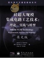
《SILICON VLSI TECHNOLOGY FUNDAMENTALS PRACTICE AND MODELING》
| 作者 | 编者 |
|---|---|
| 出版 | 未查询到或未知 |
| 参考页数 | 817 |
| 出版时间 | 没有确切时间的资料 目录预览 |
| ISBN号 | 7505386387 — 求助条款 |
| PDF编号 | 812399178(仅供预览,未存储实际文件) |
| 求助格式 | 扫描PDF(若分多册发行,每次仅能受理1册) |
Chapter 1 Introduction and Historical Perspective1
1.1 Introduction1
1.2 Integrated Circuits and the Planar Process—Key Inventions That Made It All Possible7
1.3 Semiconductors13
1.4 Semiconductor Devices33
1.4.1 PN Diodes33
1.4.2 MOS Transistors36
1.4.3 Bipolar Junction Transistors39
1.5 Semiconductor Technology Families41
1.6 Modern Scientific Discovery—Experiments, Theory, and Computer Simulation43
1.7 The Plan For This Book45
1.8 Summary of Key Ideas46
1.9 References46
1.10 Problems47
Chapter 2 Modern CMOS Technology49
2.1 Introduction49
2.2 CMOS Process How50
2.2.1 The Beginning—Choosing a Substrate51
2.2.2 Active Region Formation52
2.2.3 Process Option for Device Isolation—Shallow Trench Isolation57
2.2.4 N and P Well Formation60
2.2.5 Process Options for Active Region and Well Formation63
2.2.6 Gate Formation71
2.2.7 Tip or Extension (LDD) Formation76
2.2.8 Source/Drain Formation80
2.2.9 Contact and Local Interconnect Formation82
2.2.10 Multilevel Metal Formation84
2.3 Summary of Key Ideas90
2.4 Probems91
Chapter 3 Crystal Growth, Wafer Fabrication and Basic Properties of Silicon Wafers93
3.1 Introduction93
3.2 Historical Development and Basic Concepts93
3.2.1 Crystal Structure94
3.2.2 Defects in Crystals97
3.2.3 Raw Materials and Purification101
3.2.4 Czochralski and Float-Zone Crystal Growth Methods102
3.2.5 Wafer Preparation and Specification105
3.3 Manufacturing Methods and Equipment109
3.4 Measurement Methods111
3.4.1 Electrical Measurements111
3.4.1.1 Hot Point Probe112
3.4.1.2 Sheet Resistance113
3.4.1.3 Hall Effect Measurements115
3.4.2 Physical Measurements117
3.4.2.1 Defect Etches117
3.4.2.2 Fourier Transform Infrared Spectroscopy (FTIR)118
3.4.2.3 Electron Microscopy119
3.5 Models and Simulation121
3.5.1 Czochralski Crystal Growth122
3.5.2 Dopant Incorporation during CZ Crystal Growth125
3.5.3 Zone Refining and FZ Growth128
3.5.4 Point Defects131
3.5.5 Oxygen in Silicon138
3.5.6 Carbon in Silicon142
3.5.7 Simulation143
3.6 Limits and Future Trends in Technologies and Models144
3.7 Summary of Key Ideas146
3.8 References147
3.9 Problems148
Chapter 4 Semiconductor Manufacturing—Clean Rooms, Wafer Cleaning,and Gettering151
4.1 Introduction151
4.2 Historical Development and Basic Concepts154
4.2.1 Level 1 Contamination Reduction: Clean Factories157
4.2.2 Level 2 Contamination Reduction: Wafer Cleaning159
4.2.3 Level 3 Contamination Reduction: Gettering161
4.3 Manufacturing Methods and Equipment165
4.3.1 Level 1 Contamination Reduction: Clean Factories165
4.3.2 Level 2 Contamination Reduction: Wafer Cleaning166
4.3.3 Level 3 Contamination Reduction: Gettering167
4.4 Measurement Methods169
4.4.1 Level 1 Contamination Reduction: Clean Factories169
4.4.2 Level 2 Contamination Reduction: Wafer Cleaning173
4.4.3 Level 3 Contamination Reduction: Gettering176
4.5 Models and Simulation180
4.5.1 Level 1 Contamination Reduction: Clean Factories181
4.5.2 Level 2 Contamination Reduction: Wafer Cleaning184
4.5.3 Level 3 Contamination Reduction: Gettering186
4.5.3.1 Step 1: Making the Metal Atoms Mobile186
4.5.3.2 Step 2: Metal Diffusion to the Gettering Site187
4.5.3.3 Step 3: Trapping the Metal Atoms at the Gettering Site190
4.6 Limits and Future Trends in Technologies and Models193
4.7 Summary of Key Ideas196
4.7 References196
4.9 Problems198
Chapter 5 Lithography201
5.1 Introduction201
5.2 Historical Development and Basic Concepts203
5.2.1 Light Sources206
5.2.2 Wafer Exposure Systems208
5.2.2.1 Optics Basics—Ray Tracing and Diffraction209
5.2.2.2 Projection Systems (Fraunhofer Diffraction)212
5.2.2.3 Contact and Proximity Systems (Fresnel Diffraction)219
5.2.3 Photoresists221
5.2.3.1 g-line and i-line Resists223
5.2.3.2 Deep Ultraviolet (DUV) Resists225
5.2.3.3 Basic Properties and Characterization of Resists227
5.2.4 Mask Engineering—Optical Proximity Correction and Phase Shifting230
5.3 Manufacturing Methods and Equipment234
5.3.1 Wafer Exposure Systems234
5.3.2 Photoresists238
5.4 Measurement Methods241
5.4.1 Measurement of Mask Features and Defects242
5.4.2 Measurement of Resist Patterns244
5.4.3 Measurement of Etched Features244
5.5 Models and Simulation246
5.5.1 Wafer Exposure Systems247
5.5.2 Optical Intensity Pattern in the Photoresist253
5.5.3 Photoresist Exposure259
5.5.3.1 g-line and i-line DNQ Resists259
5.5.3.2 DUV Resists263
5.5.4 Postexposure Bake (PEB)264
5.5.4.1 g-line and i-line DNQ Resists264
5.5.4.2 DUV Resists266
5.5.5 Photoresist Developing267
5.5.6 Photoresist Postbake270
5.5.7 Advanced Mask Engineering271
5.6 Limits and Future Trends in Technologies and Models272
5.6.1 Electron Beam Lithography273
5.6.2 X-ray Lithography275
5.6.3 Advanced Mask Engineering277
5.6.4 New Resists278
5.7 Summary of Key Ideas281
5.8 References281
5.9 Problems283
Chapter 6 Thermal Oxidation and the Si/SiO2 Interface287
6.1 Introduction287
6.2 Historical Development and Basic Concepts290
6.3 Manufacturing Methods and Equipment296
6.4 Measurement Methods298
6.4.1 Physical Measurements299
6.4.2 Optical Measurements299
6.4.3 Electrical Measurements—The MOS Capacitor301
6.5 Models and Simulation312
6.5.1 First-Order Planar Growth Kinetic —The Linear Parabolic Model313
6.5.2 Other Models for Planar Oxidation Kinetics322
6.5.3 Thin Oxide SiO2 Growth Kinetics326
6.5.4 Dependence of Growth Kinetics on Pressure328
6.5.5 Dependence of Growth Kinetics on Crystal Orientation329
6.5.6 Mixed Ambient Growth Kinetics332
6.5.72D SiO2 Growth Kinetics333
6.5.8 Advanced Point Defect Based Models for Oxidation339
6.5.9 Substrate Doping Effects343
6.5.10 Polysilicon Oxidation345
6.5.11 Si3N4 Growth and Oxidation Kinetics347
6.5.12 Silicide Oxidation350
6.5.13 Si/SiO2 Interface Charges352
6.5.14 Complete Oxidation Module Simulation357
6.6 Limits and Future Trends in Technologies and Models359
6.7 Summary of Key Ideas361
6.8 References361
6.9 Problems364
Chapter 7 Dopant Diffusion371
7.1 Introduction371
7.2 Historical Development and Basic Concepts374
7.2.1 Dopant Solid Solubility375
7.2.2 Diffusion from a Macroscopic Viewpoint377
7.2.3 Analytic Solutions of the Diffusion Equation379
7.2.4 Gaussian Solution in an Infinite Medium380
7.2.5 Gaussian Solution Near a Surface381
7.2.6 Error-Function Solution in an Infinite Medium382
7.2.7 Error-Function Solution Near a Surface384
7.2.8 Intrinsic Diffusion Coefficients of Dopants in Silicon386
7.2.9 Effect of Successive Diffusion Steps388
7.2.10 Design and Evaluation of Diffused Layers389
7.2.11 Summary of Basic Diffusion Concepts392
7.3 Manufacturing Methods and Equipment392
7.4 Measurement Methods395
7.4.1 SIMS396
7.4.2 Spreading Resistance397
7.4.3 Sheet Resistance398
7.4.4 Capacitance Voltage399
7.4.5 TEM Cross Section399
7.4.62D Electrical Measurements Using Scanning Probe Microscopy400
7.4.7 Inverse Electrical Measurements402
7.5 Models and Simulation403
7.5.1 Numerical Solutions of the Diffusion Equation403
7.5.2 Modifications to Fick's Laws to Account for Electric Field Effects406
7.5.3 Modifications to Fick's Laws to Account for Concentration-Dependent Diffusion409
7.5.4 Segregation413
7.5.5 Interfacial Dopant Pileup415
7.5.6 Summary of the Macroscopic Diffusion Approach417
7.5.7 The Physical Basis for Diffusion at an Atomic Scale417
7.5.8 Oxidation-Enhanced or -Retarded Diffusion419
7.5.9 Dopant Diffusion Occurs by Both I and V422
7.5.10 Activation Energy for Self-Diffusion and Dopant Diffusion426
7.5.11 Dopant-Defect Interactions426
7.5.12 Chemical Equilibrium Formulation for Dopant-Defect Interactions432
7.5.13 Simplified Expression for Modeling434
7.5.14 Charge State Effects436
7.6 Limits and Future Trends in Technologies and Models439
7.6.1 Doping Methods440
7.6.2 Advanced Dopant Profile Modeling—Fully Kinetic Description of Dopant-Defect Interactions440
7.7 Summary of Key Ideas442
7.8 References443
7.9 Problems445
Chapter 8 Ion Implantation451
8.1 Introduction451
8.2 Historical Development and Basic Concepts451
8.2.1 Implants in Real Silicon—The Role of the Crystal Structure461
8.3 Manufacturing Methods and Equipment463
8.3.1 High-Energy Implants466
8.3.2 Ultralow Energy Implants468
8.3.3 Ion Beam Heating469
8.4 Measurement Methods469
8.5 Models and Simulations470
8.5.1 Nuclear Stopping471
8.5.2 Nonlocal Electronic Stopping473
8.5.3 Local Electronic Stopping474
8.5.4 Total Stopping Powers475
8.5.5 Damage Production476
8.5.6 Damage Annealing479
8.5.7 Solid-Phase Epitaxy482
8.5.8 Dopant Activation484
8.5.9 Transient-Enhanced Diffusion486
8.5.10 Atomic-Level Understanding of TED488
8.5.11 Effects on Devices497
8.6 Limits and Future Trends in Technologies and Models499
8.7 Summary of Key Ideas500
8.8 References500
8.9 Problems502
Chapter 9 Thin Film Deposition509
9.1 Introduction509
9.2 Historical Development and Basic Concepts511
9.2.1 Chemical Vapor Deposition (CVD)512
9.2.1.1 Atmospheric Pressure Chemical Vapor Deposition (APCVD)513
9.2.1.2 Low-Pressure Chemical Vapor Deposition (LPCVD)525
9.2.1.3 Plasma-Enhanced Chemical Vapor Deposition (PECVD)527
9.2.1.4 High-Density Plasma Chemical Vapor Deposition (HDPCVD)530
9.2.2 Physical Vapor Deposition (PVD)530
9.2.2.1 Evaporation531
9.2.2.2 Sputter Deposition539
9.3 Manufacturing Methods554
9.3.1 Epitaxial Silicon Deposition556
9.3.2 Polycrystalline Silicon Deposition558
9.3.3 Silicon Nitride Deposition561
9.3.4 Silicon Dioxide Deposition563
9.3.5 Al Deposition565
9.3.6 Ti and Ti-W Deposition566
9.3.7 W Deposition567
9.3.8 TiSi2 and WSi2 Deposition567
9.3.9 TiN Deposition568
9.3.10 Cu Deposition570
9.4 Measurement Methods572
9.5 Models and Simulation573
9.5.1 Models for Deposition Simulations573
9.5.1.1 Models in Physically Based Simulators Such as SPEEDIE574
9.5.1.2 Models for Different Types of Deposition Systems582
9.5.1.3 Comparing CVD and PVD and Typical Parameter Values587
9.5.2 Simulations of Deposition Using a Physically Based Simulator, SPEEDIE590
9.5.3 Other Deposition Simulations598
9.6 Limits and Future Trends in Technologies and Models601
9.7 Summary of Key Ideas602
9.8 References603
9.9 Problems605
Chapter 10 Etching609
10.1 Introduction609
10.2 Historical Development and Basic Concepts612
10.2.1 Wet Etching612
10.2.2 Plasma Etching619
10.2.2.1 Plasma Etching Mechanisms621
10.2.2.2 Types of Plasma Etch Systems628
10.2.2.3 Summary of Plasma Systems and Mechanisms636
10.3 Manufacturing Methods637
10.3.1 Plasma Etching Conditions and Issues638
10.3.2 Plasma Etch Methods for Various Films643
10.3.2.1 Plasma Etching Silicon Dioxide644
10.3.2.2 Plasma Etching Polysilicon647
10.3.2.3 Plasma Etching Aluminum649
10.4 Measurement Methods650
10.5 Models and Simulation653
10.5.1 Models for Etching Simulation653
10.5.2 Etching Models—Linear Etch Model656
10.5.3 Etching Models—Saturation/Adsorption Model for Ion-Enhanced Etching663
10.5.4 Etching Models—More Advanced Models669
10.5.5 Other Etching Simulations671
10.6 Limits and Future Trends in Technologies and Models675
10.7 Summary of Key Ideas676
10.8 References677
10.9 Problems679
Chapter 11 Back-End Technology681
11.1 Introduction681
11.2 Historical Development and Basic Concepts687
11.2.1 Contacts688
11.2.2 Interconnects and Vias695
11.2.3 Dielectrics707
11.3 Manufacturing Methods and Equipment715
11.3.1 Silicided Gates and Source/Drain Regions716
11.3.2 First-level Dielectric Processing718
11.3.3 Contact Formation719
11.3.4 Global Interconnects721
11.3.5 IMD Deposition and Planarization723
11.3.6 Via Formation724
11.3.7 Final Steps725
11.4 Measurement Methods725
11.4.1 Morphological Measurements726
11.4.2 Electrical Measurements726
11.4.3 Chemical and Structural Measurements732
11.4.4 Mechanical Measurements734
11.5 Models and Simulation737
11.5.1 Silicide Formation738
11.5.2 Chemical-Mechanical Polishing744
11.5.3 Reflow746
11.5.4 Grain Growth753
11.5.5 Diffusion in Polycrystalline Materials762
11.5.6 Electromigration765
11.6 Limits and Future Trends in Technologies and Models776
11.7 Summary of Key Ideas780
11.8 References781
11.9 Problems784
Appendices787
A.l Standard Prefixes787
A.2 Useful Conversions787
A.3 Physical Constants788
A.4 Physical Properties of Silicon788
A.5 Properties of Insulators Used in Silicon Technology789
A.6 Color Chart for Deposited Si3N4 Films Observed Perpendicularly under Daylight Fluorescent Lighting789
A.7 Color Chart for Thermally Grown SiO2 Films Observed Perpendicularly under Daylight Fluorescent Lighting790
A.8 Irwin Curves791
A.9 Error Function793
A.10 List of Important Symbols797
A.11 List of Common Acronyms798
A.12 Tables in Text801
A.13 Answers to Selected Problems802
Index805
《SILICON VLSI TECHNOLOGY FUNDAMENTALS PRACTICE AND MODELING》由于是年代较久的资料都绝版了,几乎不可能购买到实物。如果大家为了学习确实需要,可向博主求助其电子版PDF文件。对合法合规的求助,我会当即受理并将下载地址发送给你。
高度相关资料
-
- ADHESION AND ADHESIVES FUNDAMENTALS AND PRACTICE
- SOCIETY OF CHEMICAL INDUSTRY
-

- TRANSMISSION ELECTRON MICROSCOPY OF SILICON SILICON VLSI CIRCUITS AND STRUCTURES
- 1983 A WILEY-INTERSCIENCE PUBLICATION
-

- POBOTIC TECHNOLOGY PRINCIPLES AND PRACTICE
- 1986 Van Nostrand Reinhold Company Inc
-

- CONCRETE TECHNOLOGY AND PRACTICE
- 1965 ANGUS AND ROBERTSON
-

- CONCRETE TECHNOLOGY THEORY AND PRACTICE
- 1982 S.CHAND & COMPANY LTD.
-

- combustion physical and chemical fundamentals modeling and simmulation experiments pollutan
- prof. dr. dr. h. c.
-

- FUNDAMENTALS OF TURBULENCE MODELING
- 1998 TRYLOR&FRANCIS
-
- SEMICONDUCTOR DEVICE MODELING FOR VLSI
- 1993 PRENTICE HALL
-
- VLSI Technology Fundamentals and Applications
- 1986 Springer-Verlag Berlin Heidelberg
-

- Electrical Installation Technology And Practice
- 1964 The English Language Book Society
-

- Catalytic Ammonia Synthesis Fundamentals and Practice
- 1991 PLENUM PRESS
提示:百度云已更名为百度网盘(百度盘),天翼云盘、微盘下载地址……暂未提供。➥ PDF文字可复制化或转WORD
