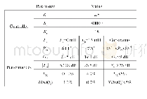
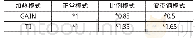
《Table 2 Controller Parameters》
 提示:宽带有限、当前游客访问压缩模式
本系列图表出处文件名:随高清版一同展现
《Systematic design method for PI controller with Virtual Resistor-based Active Damping of LCL filter》
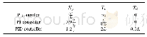
Fig.2 shows the timing diagram of the implemented VOC with VR-AD that presents the PWM references sampling and update instants and the execution time of the different aforementioned modules.As shown in this figure,the input variables Vdc,Vg(a,b,c),i2(a,b,c)and ic(a,b,c)are sampled at higher carrier vertexes,while the converter voltage vector is updated.Consequently,the time delay is equal to the sampling period Ts.In Fig.2,tPI_Vdc,tθdq,tPI_i2,tVR-AD and tPWM are the execution time of the respective modules:DC-link voltage control module,grid synchronization module,grid currents regulation module,VR-AD module and PWM module.Table 1 shows the system and LCL filter parameters.Also,tAD and Tex are,respectively,the A/D conversion time and the execution time.
| 图表编号 | XD0020049400 严禁用于非法目的 |
|---|---|
| 绘制时间 | 2018.08.01 |
| 作者 | Marwa Ben Sad-Romdhane、Mohmed Wissem Naouar、Ilhem Slama-Belkhodja |
| 绘制单位 | Université de Tunis El Manar, Ecole Nationale d'Ingénieurs de Tunis, LR 11 ES 15, Laboratoire des Systèmes Electriques、Université de Tunis El Manar, Ecole Nationale d'Ingénieurs de Tunis, LR 11 ES 15, Laboratoire des Systèmes Electriques、Université de T |
| 更多格式 | 高清、无水印(增值服务) |