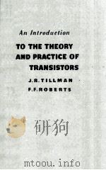
《AN INTRODUCTION TO THE THEORY AND PRACTICE OF TRANSISTORS》求取 ⇩
| 作者 | J.R. TILLMAN AND F.F. ROBERTS 编者 |
|---|---|
| 出版 | 未查询到或未知 |
| 参考页数 | ✅ 真实服务 非骗流量 ❤️ |
| 出版时间 | 没有确切时间的资料 目录预览 |
| ISBN号 | 无 — 违规投诉 / 求助条款 |
| PDF编号 | 820349608(学习资料 勿作它用) |
| 求助格式 | 扫描PDF(若分多册发行,每次仅能受理1册) |
PART 1THE THEORETICAL BACKGROUND:THE PHYSICS OF SEMICONDUCTORS AND TRANSISTORS1
1.The Relevant Basic Properties of Semiconductors3
1.1.Electrical conduction due to all types of mobile particles3
1.2.Wave-mechanical description of the extra-nuclear electronic states of the atom4
1.3.Wave-mechanics of electrons in a crystal7
1.4.Occupation of allowed states in the conduction and valence bands11
1.5.Occupation of allowed states in the forbidden band22
1.6.Nature of ordinary donor and acceptor states26
1.7.Mobility of the carriers28
1.8.Further considera-tion of effective masses and energy gaps38
1.9.The life-times of electrons in the conduction band and of holes in the valence band47
1.10.The steady-state lifetimes53
1.11.The small-signal transient lifetimes58
1.12.The large-signal transient lifetimes60
1.13.Direct photon-radiative recombination62
1.14.Surface recombination63
1.15.Non-recombination traps in bulk germanium and silicon68
1.16.References70
2.The p-n Junction72
2.1.The p-n junction without external bias72
2.2.Digression on imrefs and diffusion80
2.3.The p-n junc-tion with reverse bias83
2.4.The p-n junction with forward bias87
2.5.References91
3.The Minority Carrier Junction Transistor92
3.1.Fundamental relationships between the currents and voltages of a pair of p-n junctions arbitrarily loca-ted on a uniformly n-type or p-type material92
3.2.Magnitudes and frequency-dependences of the admit-tances for two simplified transistor structures105
3.3.Expression of the static characteristics of the ideal transistor in terms of the circuit e.m.f.s instead of terminal voltages109
3.4.Departures from the ideal tran-sistor due to series resistances and junction capacit-ances110
3.5.Departures from the ideal transistor due to the voltage-dependence of base-width115
3.6.Punch-through,Zener and avalanche effects117
3.7.High-current effects124
3.8.The effects of a graded resistivity in the base region125
3.9.References129
PART 2PRACTICE:TECHNOLOGY,PROPERTIES AND APPLICATIONS131
4.Technology133
4.1.The preparation of semiconductors for diodes and transistors133
4.1.1.Introduction131
4.1.2.The preparation of germanium131
4.1.3.The preparation of silicon140
4.2.The fabrication of point devices144
4.2.1.Point-contact diodes144
4.2.2.Point-contact transistors146
4.3.Junction techniques and devices150
4.3.1.Grown junctions and grown transistors-Dope growing-Rate growing150
4.3.2.The melt-back and melt-quench techniques154
4.3.3.The alloying technique157
4.3.4.The surface-barrier tran-sistor165
4.3.5.Diffusion techniques and diffused devices-Diffusion-Diffused diodes-Diffused transistors166
4.3.6.Mixed techniques173
4.3.7.A comparison of the various techniques177
4.4.References178
5.The Electrical Properties of Transistors and of Semicon-ductor Diodes and their Measurement179
5.1.Diodes179
5.1.1.Silicon point-contact diodes179
5.1.2.Germanium point-contact diodes181
5.1.3.Low-and medium-power junction diodes186
5.1.4.High-power junction diodes188
5.1.5.Voltage-reference diodes189
5.1.6.Other diodes190
5.2.Point-contact transistors193
5.3.Junction transistors198
5.3.1.Early observations198
5.3.2.Representation as a circuit element200
5.3.3.Improved equivalent circuits204
5.3.4.The variation of parameters with bias conditions and temperature209
5.3.5.The variation of current gain with frequency217
5.3.6.The distinction between a and α and their depen-dence on frequency220
5.3.7.The maximum frequency of oscillation221
5.3.8.Deducing the structure from the para-meters222
5.4.Thermal runaway223
5.5.The noise pro-perties of transistors225
5.6.The transient response and large-signal behaviour of junction transistors229
5.7.The measurement of the properties of junction tran-sistors234
5.8.Photo devices240
5.9.References244
6.Applications246
6.1.Applications of semiconductor diodes246
6.2.Applications of transistors:limitations imposed by the transistor parameters and methods of control250
6.2.1.Limitations set by the direct-current properties-The collector leakage current and d.c.stabilization-The maximum permissible collector voltage-The collector voltage at saturation251
6.2.2.Limitations set by the dynamic properties-The dependence of current gain on frequency-The input and output impedances-The base resistance and collector capacitance-Neutraliza-tion and unilateralization261
6.2.3.Other limitations of junction transistors266
6.2.4.The limitations of point-contact transistors267
6.3.Applications of point-contact transistors268
6.4.The junction transistor as an amplifier273
6.4.1.Small-signal amplifiers-The common-base cir-cuit-The common-emitter circuit-The common-col-lector circuit-The cascading of amplifying stages273
6.4.2.Large-signal amplifiers290
6.5.Oscillators and direct-current converters,using junction transistors295
6.5.1.General295
6.5.2.Negative-resistance oscillators299
6.5.3.Feedback oscillators301
6.5.4.Direct-current con-verters309
6.6.Switching applications of junction transis-tors313
6.6.1.General313
6.6.2.Some non-regenerative switching circuits314
6.6.3.Some regenerative switching circuits-General-Circuits based on symmetrical con-figurations-Asymmetrical configurations using two transistors-Blocking oscillators321
6.6.4.The generation of sawtooth waveforms331
6.7.References335
Index337
《AN INTRODUCTION TO THE THEORY AND PRACTICE OF TRANSISTORS》由于是年代较久的资料都绝版了,几乎不可能购买到实物。如果大家为了学习确实需要,可向博主求助其电子版PDF文件。对合法合规的求助,我会当即受理并将下载地址发送给你。
高度相关资料
-

- THE NEW RIGHT IN BRITAIN AN INTRODUCTION TO THEORY AND PRACTICE
- 1994 PLUTO PRESS
-
- AN INTRODUCTION TO THE THEORY OF COMPUTATION
- 1989 COMPUTER SCIENCE PRESS
-
- AN INTRODUCTION TO THE THEORY OF SEISMILOGY
- 1963 CAMBRIDGE UNIV PR
-
- An Introduction To The Theory of Numbers
- 1955 Pergmon Press
-
- EDTA TITRATIONS AN INTRODUCTION TO THE THEORY AND PRACTICE
- 1959 PERGAMON PRESS
-

- AN INTRODUCTION TO THE THEORY OF RELATIVITY
- 1964 BUTTERWORTHS
-
- AN INTRODUCTION TO THE THEORY OF VALUE
- 1931 MACMILLAN AND CO.
-
- An introduction to the general theory of algorithms
- 1978 NorthHolland
-
- AN INTRODUCTION TO THE THEORY OF ELASTICITY
- 1980 LONGMAN
-
- AN INTRODUCTION TO THE THEORY OF RELATIVITY
- 1964 LONDON BUTTER WORTHS
提示:百度云已更名为百度网盘(百度盘),天翼云盘、微盘下载地址……暂未提供。➥ PDF文字可复制化或转WORD
